Introduction
A single failed PCB can take down a hospital infusion pump, an automotive module, or an industrial controller. Even well-built boards develop faults over time from thermal stress, vibration, and design gaps. In many electronics programs, board-level failures remain one of the most common causes of field returns and debug delays.
Many engineers and technicians hit the same wall: a board fails, and troubleshooting turns into guesswork. Aging components, weak solder joints, environmental exposure, and handling damage are usually behind it.
You don't need a lab full of exotic equipment to find and fix most faults. This guide breaks PCB testing and troubleshooting into a simple 7-step process, from visual inspection through validated repair. It also covers when fixing a board makes more sense than replacing it.
Whether you're debugging a single prototype or chasing down a returned production unit, this framework helps you isolate the real problem instead of chasing symptoms.
Key Takeaways
- Most PCB failures trace back to shorts, opens, component failure, or contamination—not obscure root causes
- Repair-versus-replace decisions hinge on fault severity, board maturity, and real repair cost
- A structured 7-step process isolates faults faster and cuts unnecessary part swaps
- Complex, high-density, or regulated boards warrant professional-grade test gear and ISO-certified processes
What Is PCB Testing & Troubleshooting?
PCB testing verifies a board's electrical, functional, and physical integrity against its design specifications. It's a pass/fail exercise that answers one question: does this board perform the way it was designed to?
Troubleshooting is different. It's the diagnostic process of isolating and correcting the root cause once a fault has already been detected. Testing tells you something is wrong. Troubleshooting tells you why.
Here's the part many teams overlook: a board that passed initial qualification isn't guaranteed to stay that way. PCBs are systems that degrade under real-world stress:
- Thermal cycling weakens solder joints through repeated heating and cooling
- Vibration accelerates fatigue in already-stressed connections
- Moisture and airborne contaminants create slow, corrosive damage over months or years
A NASA study on ball grid array assemblies found that combined thermal cycling and vibration cut cycles-to-failure by more than 50% compared with thermal cycling alone (NASA Technical Reports Server). That's why periodic testing matters, even for boards that looked flawless on day one.
Common PCB Problems & Root Causes
Most PCB failures follow a handful of predictable patterns tied to soldering quality, component behavior, or design shortcuts. Spotting the pattern early speeds up everything that follows.
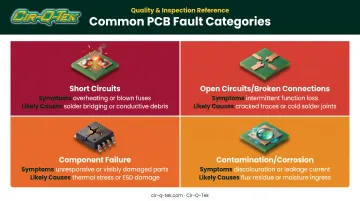
Short Circuits
Symptoms: Overheating components, unexpected shutdowns, blown fuses, or a supply rail that collapses under load.
Likely causes: Solder bridging between adjacent pads, copper trace contact from misaligned layers, or plating voids that let conductors touch under load. Kester's defect research points to stencil misalignment, excess solder paste, and slow preheat as common contributors to bridging.
Open Circuits / Broken Connections
Symptoms: Intermittent function, complete signal loss, a board that works only when you press on it.
Likely causes: Cracked traces from flexing, poor soldering that never made full contact, or physical damage during handling. Clogged stencil apertures and lead coplanarity issues can also leave a joint with no real connection at all.
Component Failure
Symptoms: Erratic behavior, or no output from a specific circuit block.
Likely causes: Thermal stress over repeated cycles, an incorrect value slipped into assembly, ESD damage at handling, or aging on capacitors and connectors. A part that worked at bring-up and fails later often points to thermal or electrical overstress rather than a bad solder joint.
Contamination & Corrosion
Symptoms: Gradual performance decline, visible residue, discoloration around joints or pads.
Likely causes: Ionic flux residue left after soldering, humidity exposure, or inadequate post-assembly cleaning. Moisture plus ionic contamination can form conductive paths through electrochemical migration, a common driver of surface-insulation-resistance failures in the field (Indium Corporation).
The 7-Step Process to Test & Troubleshoot a PCB
Jumping straight to repairs without a structured process wastes time and often misses the true root cause. This 7-step framework moves from basic inspection to validated repair, and it applies equally to a one-off prototype or a batch of production boards.
Step 1: Conduct a Visual Inspection
Start here every time. Look for cracked, discolored, or swollen components and any sign of heat damage on the board surface.
- Check pins, connectors, and solder joints for bending, corrosion, or bridging
- Use magnification or automated optical inspection (AOI) for dense, fine-pitch boards where defects hide between components
Step 2: Test Power and Continuity
Use a multimeter or continuity tester before you power anything up. Check for shorts and open circuits along traces and connectors.
- Verify voltage at key test points before applying full power
- Flag abnormal resistance or continuity readings for deeper investigation later
Skipping this step is how technicians fry a board that had a simple, fixable short.
Step 3: Identify the Fault Category
Classify what you're looking at. This single decision determines which advanced test method you'll use next:
- Mechanical
- Electrical/component
- Design-related
- Environmental
Rule out external factors first, such as a faulty power supply or a bad input signal feeding the board. A board that "fails" because of a dying bench supply isn't actually a board problem, and misdiagnosing it wastes hours.
Step 4: Apply Targeted Electrical and Structural Test Methods
Once you know the fault category, match it to the right test method.
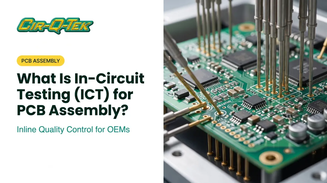
- In-Circuit Testing (ICT) isolates individual faulty components on mature, high-volume designs where a custom fixture is already cost-justified
- Flying Probe Testing suits prototypes or low-volume boards, since it uses software-controlled probes instead of a fixed bed-of-nails setup (Keysight)
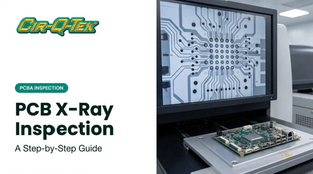
- X-ray inspection (AXI) checks hidden solder joints under BGA, QFN, or CSP packages that no optical method can see
If you don't have this equipment in-house, a turnkey PCBA partner can fill the gap.
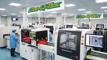
Cir-Q-Tek's SMT lines run inline AOI and X-ray inspection on every board as standard. That catches hidden joints on fine-pitch BGAs down to 0.2mm spacing without a separate inspection step.
Step 5: Run Functional and Power-On Testing
Power the board and exercise it through its intended operating conditions and full load range.
- Monitor output signals, response times, and thermal behavior for anomalies
- Compare results against original design benchmarks to confirm a clear pass or fail
A board can pass every continuity check and still misbehave once it's actually doing its job. This step catches that.
Step 6: Repair or Rework the Identified Fault
Repair the confirmed faults:
- Reflow or replace faulty solder joints
- Swap out failed components
- Repair damaged traces where feasible
- Reset or reprogram firmware if the fault is control-related rather than physical
Follow IPC-standard rework procedures, such as those in IPC-7711/7721, to avoid introducing a second defect while fixing the first one.
Step 7: Re-Test and Validate the Fix
Never skip this step. Repeat the relevant tests from Steps 2 through 5 to confirm the fault is truly gone, not just hidden.
- Run the board under both normal and peak conditions to check for recurrence
- Document everything: what failed, what you changed, and how it was verified
For medical and automotive boards, this documentation isn't optional. It's the traceability record that proves the fix met ISO 13485 or IATF 16949 requirements.
Fix vs Replace: When Should You Repair a PCB or Swap It Out?
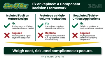
Not every fault is worth fixing. Weigh repair cost, risk, and long-term reliability against the cost of a clean replacement before you commit hours to rework.
Scenario 1: Isolated Fault on a Mature Design
Fix: A single component failure on a board that's otherwise stable and well-tested. One bad capacitor doesn't justify scrapping a proven design.
Replace: Multiple recurring failures across units, which usually points to a systemic design or batch defect rather than a one-off mistake.
Scenario 2: Prototype vs High-Volume Production
Fix: A prototype with a correctable design flaw, before tooling is locked and while changes are still cheap.
Replace: A production board where repair cost approaches the price of a redesigned, quick-turn replacement. When speed matters, a supplier that builds prototypes in 3 days and ships in 2 keeps you from waiting weeks to validate a fix.
Scenario 3: Regulated or Safety-Critical Applications
Fix: A minor, well-documented repair completed within approved quality procedures.
Replace: Any fault affecting compliance traceability or safety on medical or automotive boards. Under ISO 13485 and IATF 16949, that documentation trail matters as much as the repair itself.
If repair cost, failure risk, or compliance exposure rivals a new board, replace it. Otherwise, a controlled fix is usually the smarter path.
Common Mistakes to Avoid & Preventive Best Practices
Bad troubleshooting habits cost more in downtime and rework than the original fault ever did.
Common Mistakes to Avoid
- Treating surface symptoms instead of confirming the true root cause first
- Skipping re-testing after a repair, letting the same fault slip through to the field
- Using incompatible or out-of-spec replacement components during rework
Preventive Best Practices
- Schedule regular inspections and periodic functional re-testing for boards already in service
- Build Design for Testability (DFT) features—such as accessible test points—into the layout, not after
- Train staff on handling, ESD protocols, and documentation procedures
- Maintain proper operating conditions once boards are deployed
Frequently Asked Questions
What are the different methods for testing a printed circuit board?
The main methods are visual inspection, In-Circuit Testing (ICT), flying probe testing, AOI, X-ray inspection, and functional testing. Manufacturers typically combine several methods for full fault coverage.
Can a faulty PCB always be repaired, or does it sometimes need replacing?
Many faults are repairable, but severity, board maturity, and true repair cost determine whether repair or replacement makes more sense. Widespread damage or recurring failures usually favor replacement.
What tools do I need to start troubleshooting a PCB?
At minimum, you'll need a multimeter, a continuity tester, a magnifying inspection tool, and the board's schematic. These cover the first two or three steps of nearly any diagnosis.
How do you know if a PCB is bad?
Common signs include no power, intermittent function, a burning smell, visible damage like discoloration or swelling, and failed continuity tests. Any one of these warrants closer inspection.
What is the difference between PCB testing and PCB troubleshooting?
Testing verifies performance against design specifications and returns a pass or fail. Troubleshooting diagnoses and fixes the specific root cause behind a detected failure.
When should I bring in a professional PCB manufacturing partner instead of troubleshooting in-house?
Complex, high-density, or regulated boards benefit from professional-grade equipment like inline AOI and X-ray inspection, plus ISO-certified processes. A partner such as Cir-Q-Tek can fill gaps that in-house teams often lack.