Introduction
A flawless PCB layout means nothing if the finished board fails six months into the field. Solder joints crack. Components shift. Traces short out under load conditions nobody tested for.
That's why testing belongs in every electronics manufacturing plan. It is the checkpoint that separates a reliable product from an expensive recall. Many teams struggle to know which test method fits their project, especially when budgets are tight and timelines are tighter.
Testing has also become a compliance requirement, not just a quality preference. Medical and automotive customers increasingly demand documented verification before they'll accept a shipment.
This guide covers what PCB assembly testing is, why it matters, the main testing methods used across the industry, and how to pick the right combination for your specific project.
Key Takeaways
- Testing verifies finished boards meet electrical, functional, and quality standards before they ship
- No single method catches every defect; most manufacturers combine 2–3 for full coverage
- ICT, flying probe, AOI, X-ray, and functional testing cover the main defect types
- Match your method mix to volume, IPC reliability class, budget, and board complexity
- An ISO-certified partner with inline inspection cuts risk and rework costs
What Is PCB Assembly Testing?
PCB assembly testing is the set of inspection and electrical verification steps used to confirm a populated circuit board actually functions and was built to spec. It covers a category of processes applied at different stages for different reasons.
Testing shows up at two points in a project:
- Prototype testing — validates that the design itself works before committing to volume production
- Manufacturing testing — verifies that every unit coming off the line matches the approved design, batch after batch
Treat it as a defect-prevention gate, not a paperwork checkbox. Boards that pass on the line are far less likely to return as warranty claims or field failures.
Why Is PCB Assembly Testing Important in Electronics Manufacturing?
Testing exists to catch problems before customers do. Shorts, opens, solder bridges, tombstoned components, and misaligned parts are common in SMT assembly, and most are invisible without the right inspection method.
Skip adequate testing and here's what typically follows:
- Field failures that trigger warranty claims and damage brand reputation
- Production downtime while engineering traces a defect back to its root cause
- Costly recalls, especially in regulated industries where a single bad batch can mean a compliance investigation
The cost of catching a defect gets steeper the later you find it. NASA's Assurance Equations research describes a widely referenced 1:10:100 cost escalation model across design, fabrication, and test phases, meaning a defect caught during design costs a fraction of what the same defect costs once it reaches fabrication or test.
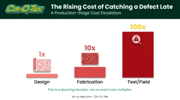
It's a planning heuristic rather than an exact multiplier for every scenario, but the direction is consistent: catching issues early is dramatically cheaper than catching them late.
Regulated Industries Treat Testing as Mandatory
Medical device and automotive customers don't treat testing as optional. The FDA's Quality Management System Regulation folds ISO 13485 requirements directly into device manufacturing oversight, and automotive OEMs operate under IATF 16949, which ties control plans and inspection data to risk and production volume.
Neither standard prescribes one specific test method. Instead, they require manufacturers to document objective evidence that the assembly meets requirements — which means your testing strategy has to be defensible, not just effective.
This is where certifications matter. Cir-Q-Tek holds ISO 9001, ISO 13485, and IATF 16949 certifications, plus a secondary quality inspection at its Pennsylvania facility before any product ships — giving medical and automotive customers a documented, auditable quality trail.
Types of PCB Assembly Testing Methods
There's no universal test that catches every defect type. Each method trades off cost, speed, and depth of coverage differently, which is why most manufacturers layer two or three together rather than betting everything on one.
In-Circuit Testing (ICT)
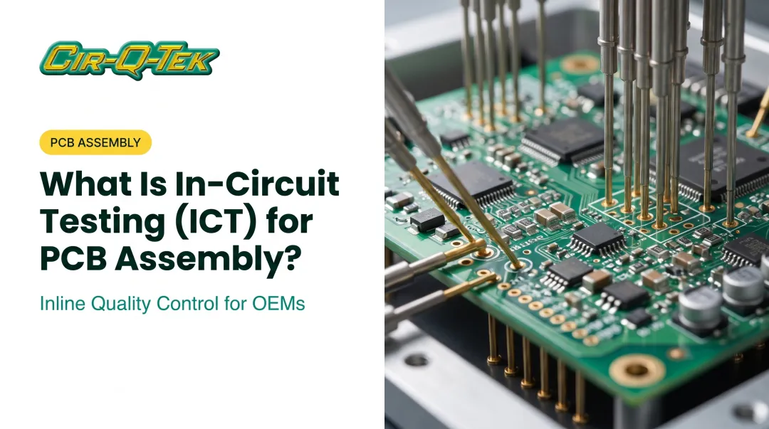
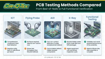
ICT uses a "bed-of-nails" fixture (a custom board loaded with spring-loaded pins) to probe individual test points and verify component values, shorts, and opens all at once.
- Strength: High fault coverage and fast per-unit test times once the fixture is built
- Limitation: Fixture tooling is expensive, making it impractical for low-volume or frequently revised boards
ICT earns its keep on mature, high-volume designs where the fixture cost gets amortized across thousands of units.
Flying Probe Testing
Flying probe testing skips the fixture entirely. Movable probes on an X-Y grid, programmed straight from CAD data, physically touch test points to check opens, shorts, resistance, and capacitance.
- Strength: No costly fixture required; test programs can be generated quickly and updated when the design changes
- Limitation: Sequential probe movement means slower per-board test times and generally lower fault detection than fixture-based ICT (KeySight)
This makes flying probe the go-to choice for prototypes and low-volume runs where boards are still evolving.
Automated Optical Inspection (AOI)
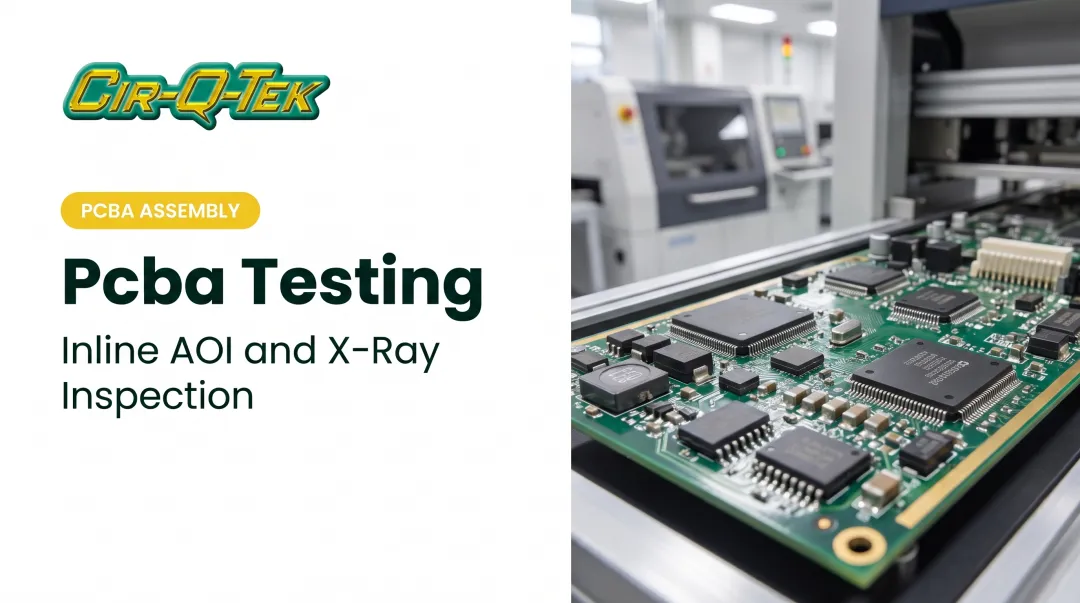
AOI uses high-resolution cameras to compare an assembled board against a "golden" reference image, flagging visible defects like solder bridges, tombstoning, skewed components, and missing parts.
- Strength: Fast, non-contact, and ideal for catching surface-level defects in real time during production
- Limitation: Can't see hidden joints under packages and doesn't confirm the board actually powers on and works
Cir-Q-Tek runs AOI as an inline system built directly into every SMT line, catching surface defects as boards move through the production flow rather than waiting for a separate post-production audit.
X-Ray Inspection
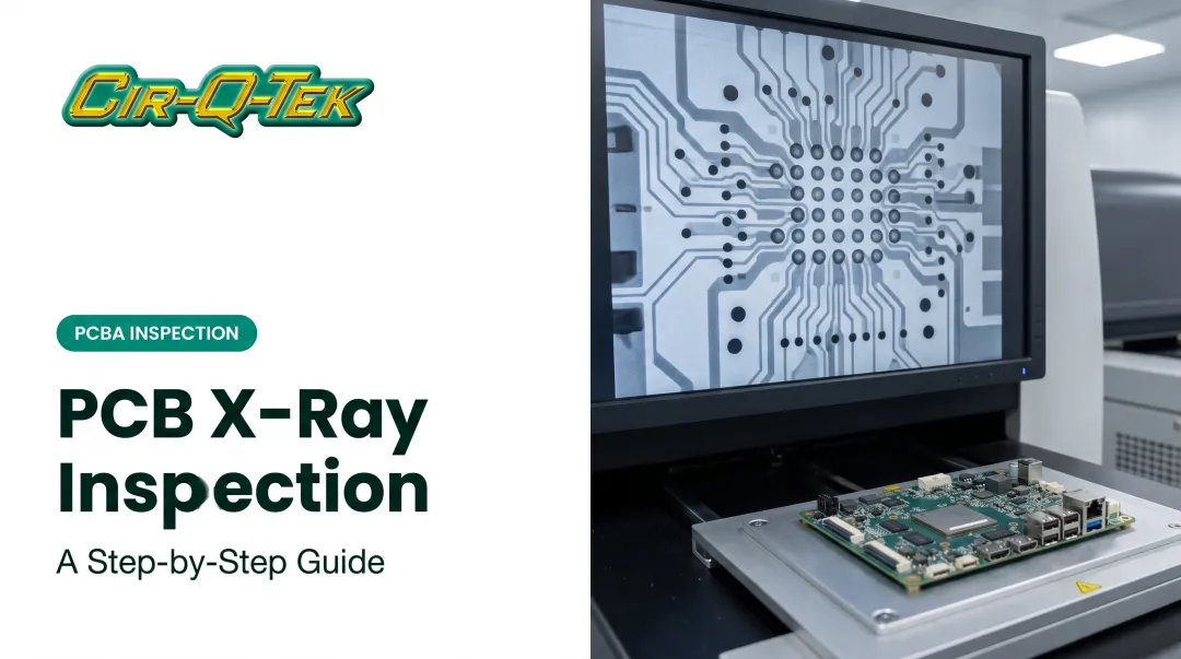
X-ray inspection images what cameras can't reach: hidden solder joints under BGAs, QFNs, and CSPs, plus internal connections in multilayer assembly structures.
- Strength: Essential for boards using fine-pitch packages where solder joints are physically invisible from above
- Limitation: Slower than AOI and requires trained operators to correctly interpret the images
Cir-Q-Tek pairs X-ray equipment with AOI on every SMT line, which matters given the facility's capability to place components as small as 01005 and BGAs spaced at 0.2mm, packages where solder joints simply can't be verified any other way.
Functional Testing
Functional testing powers the assembled board up and checks whether it actually performs according to design requirements, often simulating real-world operating conditions.
- Strength: Confirms real-world performance and catches system-level issues that structural tests miss entirely
- Limitation: Usually delivers a pass/fail result without pinpointing which component failed, and it requires custom test fixtures built for that specific board
Most production programs run functional testing last, after ICT, AOI, or X-ray have already screened for assembly-level faults.
Other Specialized Tests Worth Knowing
A few additional methods show up for specific use cases:
- Burn-in testing: runs hardware under stress for an extended period to surface early "infant mortality" failures before shipment
- ROSE testing: measures ionic contamination on the board surface; useful as a process-control tool, though it doesn't predict long-term reliability on its own
- Boundary scan testing: uses embedded test logic to check interconnects on densely packed multilayer boards without needing physical probe access
How to Choose the Right PCB Assembly Testing Method
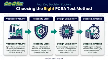
Match your test method to production volume, reliability requirements, and budget. The most advanced option is rarely the right default.
Factors to Consider
Production volume. High-volume runs justify ICT's upfront fixture cost because it pays for itself across thousands of units. Low-volume or prototype runs favor flying probe and AOI, where there's no fixture investment to recoup.
Product reliability class. IPC's classification system sets the bar for how rigorous testing needs to be:
| IPC Class | Application | Typical Testing Rigor |
|---|---|---|
| Class 1 | General consumer electronics | Basic functional verification |
| Class 2 | Dedicated-service equipment (communications, instruments) | Structural + functional testing |
| Class 3 | Mission-critical (medical, automotive, aerospace) | Full structural, functional, and documented inspection |
Design complexity. Densely packed, multilayer, or BGA-heavy boards typically need X-ray or boundary scan layered on top of standard structural testing. AOI alone won't cut it.
Budget and timeline. Weigh the upfront tooling investment against per-unit test cost and how fast you need product out the door. A $15,000 ICT fixture makes sense for a 50,000-unit run; it doesn't for a 200-unit prototype batch.
Working with a single, ISO-certified manufacturing partner simplifies a lot of this decision-making. Cir-Q-Tek runs inline AOI and X-ray inspection across every SMT line and holds ISO 9001, ISO 13485, and IATF 16949 certifications, so multiple test capabilities and compliance documentation live under one roof.
Projects that need a tailored testing plan can be scoped through a quote request with the technical team.
Common Mistakes to Avoid
- Over-engineering the test plan. Choosing the most advanced or expensive method when a simpler combination would meet requirements just adds cost without adding value.
- Relying on one method. Assuming AOI or ICT alone gives full coverage ignores that method's specific blind spots.
- Ignoring long-term costs. Fixture maintenance and retooling add up fast when a design changes mid-production. Factor that into the decision, not just the initial tooling quote.
Conclusion
PCB assembly testing determines whether your product survives contact with the real world. Treat it as a core part of the build, not a final checkbox. Each method covers a different piece of the puzzle, and most projects need at least two working together to close the gaps.
Understanding what ICT, flying probe, AOI, X-ray, and functional testing actually catch, and what they miss, puts you in a much better position to make cost-effective decisions instead of defaulting to whatever sounds most advanced.
It also helps to pick a manufacturing partner already equipped to run these tests in-house, rather than coordinating inspection across multiple vendors and risking gaps between handoffs.
Frequently Asked Questions
What is PCB assembly and testing?
PCB assembly is the process of populating a bare circuit board with components through soldering. Testing is the verification step that confirms the finished assembly is defect-free and performs to specification.
What is the difference between in-circuit testing and flying probe testing?
ICT uses a fixed bed-of-nails fixture, making it fast and cost-effective for high-volume production. Flying probe uses movable probes with no fixture, making it better suited to prototypes and low-volume runs where designs still change.
Which PCB testing method is best for prototypes or low-volume production?
Flying probe testing and AOI are typically the best fit. Both avoid the upfront fixture costs of ICT and adapt quickly when a design revision comes through.
Can AOI detect all PCB defects?
No. AOI catches visible surface defects like solder bridges and misaligned parts, but it can't verify hidden joints under BGAs or QFNs. Complementary tests like X-ray or ICT close that gap.
Does PCB testing significantly increase assembly cost?
Testing adds incremental cost, but it's small compared to what a field failure, recall, or rework cycle costs later. Catching a defect before shipment is consistently cheaper than catching it after.
Is X-ray inspection necessary for every PCB assembly?
Not always. It's most valuable for boards using BGAs, QFNs, or multilayer construction where solder joints are hidden from view. Simple, low-density boards often don't need it.