Introduction
Every circuit board has a hidden architecture: stacked layers of copper and insulation that determine whether a device works, glitches, or fails outright. As devices shrink while demanding more speed and reliability, stackup choices directly affect signal integrity, manufacturing yield, and cost.
A poorly planned stackup shows up later as crosstalk, EMI failures, or warped boards that never make it past inspection. This guide breaks down the main types of PCB stackups, how layer order actually works, and how to pick the right configuration for your project.
Key Takeaways
- PCB layers alternate copper (conductive) and dielectric (insulating) sheets; the stackup is their specific order and count
- Three core types exist: single-layer, double-layer, and multilayer/HDI, each fitting different complexity and speed needs
- Power, ground, and signal layer placement affects signal integrity and EMI just as much as total layer count
- The right stackup fits your signal requirements, volume, and budget, not the most advanced option available
- Reviewing your stackup with a certified manufacturer before fabrication prevents costly respins
What Are PCB Layers and Why Do They Matter?
A PCB layer is a sheet of copper (conductive) or dielectric material (insulating) laminated together to form a working board. The stackup is how many of these layers exist and in what order they're arranged.
Think of it like floors in a building. Each floor has a job: some carry foot traffic (signal routing), some house utilities (power distribution), and some exist purely for structural support (grounding and shielding). Stack them wrong, and the whole building underperforms.
Why Stackup Design Affects Real-World Performance
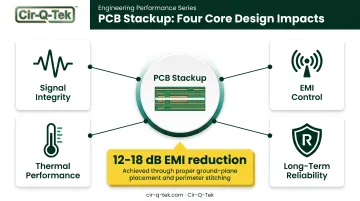
Layer arrangement directly shapes:
- Signal integrity — clean signal transmission with minimal distortion
- EMI control — how much electromagnetic noise the board radiates or absorbs
- Thermal performance — how efficiently heat spreads across the board
- Long-term reliability — resistance to warping, delamination, and fatigue
Research from EDN found that moving ground-reference planes to the outer layers and stitching them around the board's perimeter every 5mm produced a measured 12-18 dB reduction in EMI. That gap often decides whether a board passes EMI compliance testing or gets sent back for redesign.
What Goes Wrong Without Proper Planning
Skip careful stackup planning and you'll likely run into:
- Crosstalk between adjacent signal traces
- Voltage drop from inadequate power plane distribution
- Warping during lamination, especially on thinner or asymmetric builds
- Expensive, time-consuming redesigns after failed prototypes
These failures show up often when layer count is treated as an afterthought instead of an early design decision.
Types of PCB Layer Stackups
There's no universal "best" stackup. The right type depends on circuit complexity, signal speed, component density, and what you're willing to spend. Each of the three core types below solves a different problem — none of them is obsolete.
Single-Layer PCB Stackup
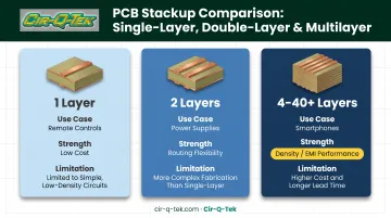
A single-layer board has one copper layer laminated onto one side of an insulating substrate, typically FR-4, with components mounted on the opposite side. There are no vias or inner layers — every trace and connection lives on one plane.
Best suited for: remote controls, basic sensors, LED drivers, and hobby projects.
Strengths:
- Lowest manufacturing cost of any construction
- Simplest design and fabrication process
- Easiest to test and repair
Limitations: minimal routing space, no dedicated power or ground plane, and it can't handle high-speed or high-density circuits.
Double-Layer PCB Stackup
Double-layer boards add a second copper layer, separated by an insulating core and connected through plated vias. This gives you double-sided component placement and considerably more routing freedom.
Best suited for: power supplies, automotive control modules, and general consumer electronics.
Strengths:
- Smaller footprint than single-layer equivalents
- More routing flexibility
- Better EMI shielding
Limitations: still no true dedicated power/ground plane separation for high-speed signals, and it can't match multilayer density.
Multilayer PCB Stackup (3+ Layers, Including HDI)
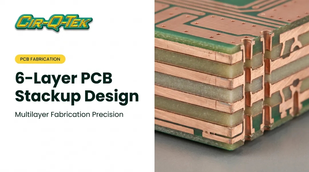
Multilayer boards stack three or more conductive layers alternating with prepreg or core dielectric, bonded through lamination. Dedicated signal, power, and ground planes sit inside the stack. Blind and buried vias, plus internal reference planes, deliver density and EMI control that single- or double-layer boards can't match.
Best suited for: smartphones, medical devices, telecom equipment, and automotive ADAS systems.
Strengths:
- Highest circuit density
- Best signal integrity and EMI performance
- Support for HDI microvias in extreme-miniaturization work
Limitations: higher cost, greater design complexity, and tighter lamination control to avoid warpage or delamination.
Manufacturers vary widely in how far they can push multilayer builds. Cir-Q-Tek, for example, fabricates multilayer PCBs up to 40 layers using laser direct imaging (LDI). LDI avoids the distortion and positional errors common with older film-based imaging.
That precision matters more as layer count climbs. Even microscopic misalignment across 40 layers can wreck via connections and impedance control.
PCB Layer Stackup Order and Composition Explained
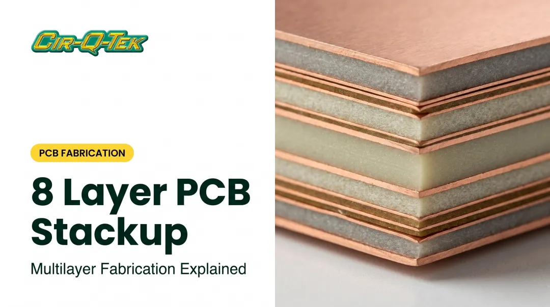
A typical multilayer stackup follows a predictable pattern from top to bottom:
- Top signal layer — outer copper for component connections
- Prepreg — uncured bonding dielectric
- Internal ground plane — shields signals, provides return path
- Core — rigid, pre-laminated dielectric
- Internal power plane — stable voltage distribution
- Additional signal layers — as needed for routing complexity
- Prepreg — bonding dielectric above the bottom layer
- Bottom signal layer
Why Power and Ground Sit in the Middle
Placing ground and power planes near the center isn't arbitrary. These internal planes shield signal layers from external EMI and give high-speed signals a stable, continuous reference path. Break that reference (for example, by routing a trace across a split plane) and return current has to detour around the gap, degrading signal quality and increasing emissions.
Core vs. Prepreg
These two materials look similar but serve different roles:
- Core is rigid, pre-laminated dielectric with copper already bonded to both sides before it enters the stackup
- Prepreg is uncured "B-stage" fiberglass that becomes hard only after hot pressing, bonding adjacent layers together during lamination
Together, they control layer separation and impedance.
Why Even Layer Counts Are the Norm
Multilayer boards almost always use an even number of layers. Symmetrical lamination, matching copper weight and construction on either side of the centerline, reduces warping and manufacturing defects. An even count makes that mirrored symmetry practical to achieve consistently.
Impedance Control Basics
Trace width, dielectric thickness, and distance to the nearest reference plane all determine characteristic impedance. Target values vary by interface rather than following one universal number. Texas Instruments specifies 90-ohm differential impedance for USB and 100-ohm differential for PCIe, SATA, and HDMI. Get the stackup geometry wrong, and you'll miss these targets no matter how good your routing is.
How to Choose the Right PCB Stackup for Your Project
The right stackup is the one that meets your requirements, not the one with the most layers. Over-engineering a board wastes money and adds lead time without improving performance.
Work through these factors in order:
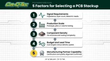
1. Signal requirements High-speed or RF designs need dedicated reference planes and typically a minimum of six layers. Low-speed digital or basic power circuits often don't.
2. Production scale A one-off prototype tolerates a pricier, more complex build. A high-volume production run makes every added layer cost multiply across thousands of units.
3. Component density Fine-pitch parts, like BGAs with 0.5mm pitch or tighter, often force a multilayer or HDI approach just to route successfully without hitting fabrication limits.
4. Budget and lead time Layer count cost isn't linear. NCAB Group's cost analysis shows increases of 26-40% at each successive jump from 2 to 4 layers, 4 to 6, and so on.
If you need a fast decision on a prototype, quick-turn options (Cir-Q-Tek offers a 3-day build with 2-day shipping) let you validate a stackup before committing to volume.
5. Manufacturing partner capability Your design is only as good as what your fabricator can actually build and verify. Look for ISO-certified processes and the inspection discipline to catch defects before they become field failures. Cir-Q-Tek backs builds with ISO 9001, ISO 13485, and IATF 16949 certification for medical and automotive-grade work, plus inline AOI and X-ray on every SMT line.
What to Check Before Finalizing Your Stackup
Before you send a design to fabrication:
- Resist over-specifying. A 12-layer HDI board isn't automatically better than a well-designed 6-layer board if the simpler option meets your specs.
- Confirm impedance and EMI targets are actually met. Don't assume adding layers solves signal problems by default.
- Check standard stackup options and tolerances against your design early. Custom builds outside standard capability often mean higher cost and longer lead time.
Conclusion
PCB layers and stackup design form the foundation of a board's performance, cost, and long-term reliability, well before a single component gets placed. Single-layer, double-layer, and multilayer constructions each solve different mixes of complexity, speed, and budget—none is inherently superior.
Understanding those tradeoffs, and reviewing your stackup with a certified manufacturer before fabrication, is what separates a smooth production run from an expensive respin. Cir-Q-Tek supports that step with ISO-certified PCB fabrication from quick-turn prototypes through multilayer production.
Frequently Asked Questions
What is layering in PCB?
Layering refers to stacking conductive copper sheets and insulating dielectric material to build a functional circuit board. Each layer is assigned a defined role: signal routing, power distribution, or grounding.
What are the typical layers of a PCB?
A typical PCB includes copper signal layers, dedicated power and ground planes, core and prepreg dielectric material, plus an outer solder mask and silkscreen layer for protection and labeling.
How many layers can a PCB have?
Commercial boards commonly range from 1 to 16 layers. Advanced manufacturers, including Cir-Q-Tek, can fabricate multilayer boards up to 40 layers depending on the application and equipment capability.
What is a PCB stackup?
A PCB stackup is the specific arrangement, order, and count of conductive and dielectric layers within a printed circuit board. It determines how signal, power, and ground layers interact.
How do I know how many layers my PCB design needs?
Signal speed, component density, and production volume are the main deciding factors. High-speed or fine-pitch designs typically need more layers; simple, low-volume circuits often don't.
Why are multilayer PCBs often designed with an even number of layers?
Even layer counts allow symmetrical lamination, matching copper and construction on both sides of the centerline. This balance reduces warping and manufacturing defects during production.