
It's become the sweet spot between cost and performance: enough layers to add dedicated power and ground planes, without the complexity (or price tag) of a 6+ layer stackup.
Before you send files to a fabricator, though, you need to understand what's actually happening inside that board. What steps go into fabrication? What drives cost up or down? Which stackup should you choose? This guide walks through all of it, plus how to vet a manufacturing partner you can trust.
Key Takeaways
- 4-layer PCBs pair 2 outer signal layers with inner power/ground planes for tighter EMI control and denser routing
- Fab flow runs inner imaging → lamination → drilling → outer imaging → solder mask → test
- Unit cost runs higher than 2-layer boards, but volume and smart stack-up choices close the gap fast
- ISO-certified partners like Cir-Q-Tek keep quality consistent on medical, automotive, and industrial builds
What Is a 4 Layer PCB?
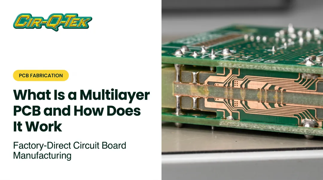
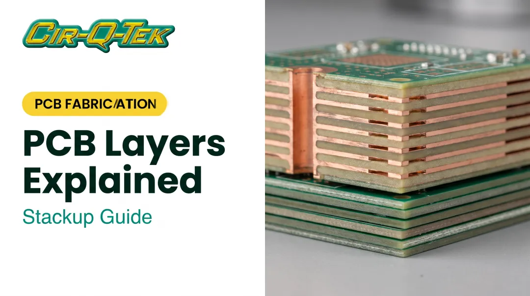
A 4-layer PCB consists of four conductive copper layers, each separated by dielectric material (typically FR4). The two outer layers carry components and signal traces. The two inner layers are usually dedicated to power and ground planes.
Why does this matter? A 2-layer board runs out of room fast once your design gets complex, forcing tight trace spacing and messy power distribution. A 6+ layer board solves that but adds cost and lead time you may not need.
The 4-layer PCB sits in the middle. It gives designers a clean ground reference, a dedicated power plane, and enough signal layers to route moderately complex circuits without over-engineering the build.
Common Stackup Configurations
Signal-Ground-Power-Signal (S-G-P-S) is the most common four-layer arrangement. The continuous ground plane sits directly beneath the top signal layer, giving high-speed traces a clean, uninterrupted return path. This setup also supports more predictable impedance control, which matters if your design includes any RF or high-speed digital signals.
Signal-Power-Ground-Signal (S-P-G-S) is a common alternative. It can support designs where the power plane needs to carry more current, but managing return paths becomes trickier, especially where routing crosses plane splits. Your fabricator's engineering team should confirm which configuration fits your specific design before locking in the stackup.

Applications Across Industries
Four-layer boards show up across a wide range of sectors:
- Medical devices — where reliability and regulatory compliance are non-negotiable
- Automotive ECUs — which need to withstand vibration, heat, and long service life
- Telecom equipment — for signal integrity in data-heavy environments
- Industrial process control — where noise immunity matters in electrically noisy plants
- Consumer electronics — balancing performance with cost
Cir-Q-Tek's ISO 13485 and IATF 16949 certifications position it to supply 4-layer boards to medical and automotive customers operating under strict regulatory oversight. Both certifications require documented quality management systems, meaning your board's fabrication history stays traceable when an auditor requests it.
The 4 Layer PCB Fabrication Process, Step by Step
Building a 4 layer board involves more steps than a simple double-sided design, since the two inner layers need to be imaged and etched before anything gets laminated together.
Step 1: Prep the laminates. Copper-clad cores are cleaned and coated with photoresist film, setting up the surface for imaging.
Step 2: Inner layer imaging. UV light exposes the circuit pattern onto the photoresist. Unwanted copper is etched away, leaving the power and ground plane patterns intact. AOI inspection checks the result against the original design data before moving forward. Catching a defect here is far cheaper than catching it after lamination.
Step 3: Lamination. Prepreg (the adhesive dielectric layer) and outer copper foils get stacked with the imaged inner core. The whole assembly is pressed under high heat and pressure, bonding all four layers into a single solid board with no trapped air or voids.
Step 4: Drilling and electroplating. Mechanical drilling creates the plated-through holes (PTH) that will electrically connect all four layers. Electroless and electrolytic copper plating then coats those hole walls, completing the interconnections.
Step 5: Outer layer imaging and etching. The same imaging and etching process from Step 2 repeats on the outer layers, forming the final circuit traces on layers 1 and 4. Copper and tin plating protect these traces during etching.
Step 6: Finishing. Solder mask goes on to protect traces from oxidation and shorts. A surface finish (HASL, ENIG, OSP, or immersion silver) is applied to the exposed copper pads. Silkscreen printing adds component labels and reference markings.
Cir-Q-Tek uses laser direct imaging (LDI) during this process instead of traditional phototool imaging. LDI eliminates distortion, shrinkage, and positional errors that can creep in with older imaging methods. That accuracy matters on a board where layer-to-layer registration directly affects reliability.

This entire sequence is governed by IPC-6012F, the qualification and performance standard for rigid printed boards released in 2023. It sets expanded requirements around copper wrap plating, internal plated layers, dielectric spacing, and hole registration: the details that separate a board that survives thermal cycling from one that delaminates six months into service.
Quality Control and Testing for 4 Layer PCBs
Fabrication accuracy is only half the story. You also need to verify the board actually works before it ships.
Electrical Testing Methods
Two methods dominate bare-board electrical verification:
- Flying probe testing — programmable probes check continuity and isolation across pads and vias. No custom fixture required, so it suits prototypes, low volume, and designs that still change often.
- Bed-of-nails testing — a custom fixture contacts many test points at once. Higher upfront tooling cost, but more economical once the design is frozen and running at volume.
Which one you need depends on where your project sits: still iterating, or locked and scaling.
Inspection Along the Way
AOI inspection at the inner-layer stage catches imaging or etching defects while the layers are still accessible, before lamination seals everything together. X-ray inspection after lamination provides a non-destructive check of hidden layer-to-layer registration, since you can no longer see those inner layers directly once the board is pressed.
Cir-Q-Tek builds AOI and X-ray inspection into its ISO 9001:2015-certified manufacturing process. Boards also receive a secondary inspection at the company's Pennsylvania facility before shipment.

How Much Does a 4 Layer PCB Cost?
A 4-layer board costs more than a comparable 2-layer design. That's not surprising once you consider what's added:
- Extra copper layers and dielectric material
- An additional lamination processing step
- Inner-layer imaging and inspection that 2-layer boards skip entirely
Exact pricing still depends on board size, quantity, materials, and turnaround time.
Volume changes the math significantly. Low-volume prototype runs carry a larger per-unit premium since setup and tooling costs get spread across fewer boards. Production volumes bring the per-unit cost down through standard economies of scale.
Cost-Saving Strategies
You have real control over your final price through design decisions:
- Optimize for manufacturability: Work with your fabricator's DFM team early, before files are finalized
- Minimize board size and via count: Fewer drilling operations and smaller panels reduce processing time
- Stick to standard thicknesses and finishes: Custom specs almost always cost more than standard options
Who builds the board affects the quote as well. Cir-Q-Tek's dual U.S.-Shenzhen office model gives you offshore manufacturing pricing with domestic-level communication and support. The company shares tariff expenses with its manufacturing partners and, in most cases, passes on a tariff reduction of more than 50% to you, listed separately on each quote.

Choosing a 4 Layer PCB Fabrication Partner
Not every fabricator handles multilayer work with the same rigor. Before committing, check these three areas.
Turnaround time. Ask about quick-turn capabilities for prototypes. Cir-Q-Tek, for example, quotes 3 days to build plus 2 days to ship for prototype samples. Production orders typically run 10 days to 4 weeks, depending on complexity.
Relevant certifications. If you're building for a regulated industry, certifications aren't optional:
- ISO 13485 for medical device manufacturing
- IATF 16949 for automotive manufacturing
Don't just take a logo on a website at face value. Confirm the certificate actually covers the fabrication site and processes involved in your project.
One-stop capabilities. A fabricator that also handles assembly (PCBA) simplifies your supply chain. Cir-Q-Tek's turnkey model integrates PCB fabrication with SMT assembly, through-hole processing, testing, and box-build. You manage one relationship instead of coordinating separate fab and assembly vendors.
Frequently Asked Questions
How much more expensive is a 4-layer PCB?
4-layer PCBs typically cost more than 2-layer boards due to extra copper, dielectric material, and an added lamination step. That price gap narrows considerably at higher production volumes.
How is a 4-layer PCB made?
A 4-layer board starts with inner layer imaging and etching, then lamination of all four layers under heat and pressure. Mechanical drilling and copper electroplating follow, then outer layer imaging, solder mask, and surface finish.
What does a 4-layer PCB mean?
A 4-layer PCB has four conductive copper layers separated by dielectric material. Two outer layers typically carry signals and components, while two inner layers serve as dedicated power and ground planes.
How many layers can a PCB have?
PCBs range from single-layer designs to 40+ layer constructions, with 4, 6, and 8 layers being the most common multilayer configurations. Cir-Q-Tek fabricates boards across this full range, including up to 40 layers, with laser direct imaging and blind/buried vias.