
This guide walks through the stackup configurations that actually get used, how to assign layers for signal integrity, what materials and thickness options look like, and what to check before you send files to a fabricator. Cir-Q-Tek manufactures multilayer PCBs up to 40 layers using laser direct imaging, which makes tight layer registration achievable even on denser 6-layer builds.
Key Takeaways
- Six layers add dedicated power/ground planes and routing capacity that 4-layer boards can't match
- No single standard stackup exists; pick the configuration based on EMC priorities versus routing density
- Layer assignment mistakes (split planes, wrong high-speed layer) cause most signal integrity failures
- Expect roughly a 30-40% cost premium over 4-layer boards, driven mainly by material and lamination
What Is a 6-Layer PCB Stackup?
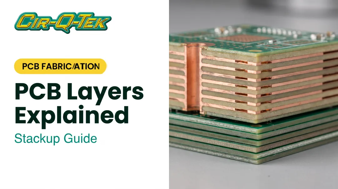
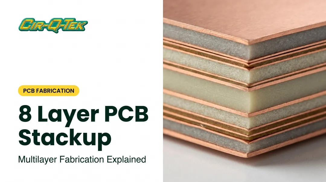
A PCB stackup is the sequential arrangement of copper, core, and prepreg layers that sets a board's electrical and mechanical behavior. Thickness, dielectric constant, and copper weight at each layer all factor into impedance and reliability.
A basic 6-layer board typically has four signal layers plus two plane layers (power and ground), separated by FR-4 core and prepreg. That's a common starting structure, not a fixed industry rule — plenty of fabricators use three signal and three plane layers instead.
When 6 Layers Make Sense
Move up from 4 layers when you're dealing with:
- High pin-count BGAs that need more breakout routing channels
- Multiple high-speed interfaces running simultaneously
- Mixed-signal designs needing isolation between analog and digital sections
- Layouts where adjacent signal traces create more crosstalk than 4 layers can control
There's no universal pin-count threshold that triggers the jump. It's a judgment call based on whether 4 layers can still provide continuous reference planes alongside enough routing space. If not, you're at 6.
Standard 6-Layer PCB Stackup Configurations
Three configurations cover most real-world 6-layer designs. Each balances routing density against signal integrity and EMC performance differently.
| Configuration (L1→L6) | Layer Mix | Best For | Trade-off |
|---|---|---|---|
| SIG/PWR/SIG/SIG/GND/SIG | 4 signal, 2 plane | Simple, low-speed boards | Weak EMC shielding; generally the least favorable option |
| SIG/GND/PWR/SIG/GND/SIG | 3 signal, 3 plane | General-purpose, mixed-signal designs | Solid reference continuity, moderate routing |
| SIG/GND/SIG/PWR/GND/SIG | 3 signal, 3 plane | High-speed, EMI-sensitive designs | Strong shielding, but fewer routing layers |
The core trade-off: more plane layers mean better continuous references and lower EMI, but fewer signal layers to route with. Design teams pick based on which constraint hurts more: routing congestion or signal integrity margin.

3 Cores vs. 2 Cores
How you laminate those layers matters as much as the order in the table. A 2-core build typically pairs inner layers on two cores with prepreg and foil making up the rest; a 3-core build uses three double-sided cores stacked with prepreg, which can tighten dielectric control between critical pairs.
When power and ground sit on adjacent layers separated by thin dielectric (core or prepreg), you gain planar capacitance between them. That capacitance supplements discrete decoupling caps and lowers spreading inductance in the PDN—especially useful on boards with fast transient current demands.
Why Symmetry Matters
Core count and plane placement only hold up if the stackup stays balanced through fab and reflow. Warping usually comes down to imbalance. To avoid bow and twist:
- Match layer count and thickness above and below the board's center
- Distribute copper evenly across layers
- Keep the stackup symmetric, not just electrically but mechanically
Tight layer-to-layer registration keeps that symmetry intact on thin-core builds. Cir-Q-Tek's laser direct imaging process supports the narrow tolerances these 6-layer configurations need between planes.

Layer Assignment and Signal Routing Guidelines
Getting the stackup right is only half the job. How you assign signals to layers determines whether the board actually performs.
Routing High-Speed Signals
Put impedance-controlled, high-speed traces on the outer layers (L1/L6), where the dielectric to the adjacent ground plane is thinnest.
- Give every critical trace an uninterrupted reference plane directly beneath it
- Never route across a plane split: it breaks the return path and invites EMI
- Prefer the outer-layer/adjacent-ground pairing for the tightest impedance control
Power Distribution Network Design
A solid PDN combines:
- A dedicated plane layer for low-impedance current delivery
- Decoupling capacitors placed close to IC power pins
- Planar capacitance from adjacent power/ground layers for high-frequency bypass when discrete caps roll off
Via Design Rules
- Place ground return vias near signal layer transitions to maintain a clean return path
- Consider backdrilling for high-speed signals above 3 Gbps, where via stubs become transmission-line loss sources (a tighter threshold than the commonly cited 3 GHz rule of thumb)
- Avoid unnecessary via stubs on any transition carrying fast edge rates
Crosstalk and Length Matching
The classic 3W rule (spacing at least 3x trace width) is a conservative starting point for crosstalk control. In practice, 1.5W to 2W spacing can work fine depending on trace width and dielectric thickness — validate with a field solver rather than assuming the rule blindly.
For differential pairs, there's no universal length-matching number. The real limit is whatever residual timing skew your interface spec allows after accounting for jitter.
Even with solid spacing and matching rules, a few layout choices still drive most respins:
- Splitting reference planes under high-speed traces
- Routing critical signals on inner layers away from adjacent ground
- Over-constraining impedance tolerance beyond what the interface actually needs

Materials, Thickness, and Cost Considerations
Thickness Options
Standard 6-layer boards run from roughly 1.0mm to 2.4mm, with 1.6mm as the most common default. Go thicker for mechanical rigidity in larger boards, or thinner for space-constrained enclosures — but confirm your fabricator's actual available constructions before locking in a target impedance.
Material Trade-offs
| Material | Properties | When to Use |
|---|---|---|
| Standard FR-4 | Low cost, adequate for most digital designs | Default choice unless a specific requirement says otherwise |
| High-Tg FR-4 | Higher thermal stability (Tg ~180°C) | Boards facing thermal cycling or lead-free reflow stress |
| Rogers/RF laminate | Stable dielectric constant, low loss at high frequency | RF and microwave circuits where FR-4's losses are unacceptable |
What Drives Cost Up
High-Tg and RF laminates raise material cost on their own. Moving from 4 to 6 layers typically adds another 30-40% to overall board cost, according to fabrication cost data from Sierra Circuits. Beyond layer count, price climbs further when you add:
- Blind or buried vias that require extra drilling and lamination steps
- Tight controlled-impedance specs that need additional verification
- Quick-turn scheduling that compresses production time
- Non-standard copper weights or unusual material stacks

Cir-Q-Tek sources 6-layer builds through its Shenzhen manufacturing network, which brings offshore pricing while keeping quality inspection domestic at its Pennsylvania facility before shipment.
Applications and Choosing a Manufacturing Partner
Six-layer boards fit applications where routing density and signal isolation both matter:
- Networking/telecom — high-speed interfaces plus dense connector breakout
- Industrial control — mixed analog/digital signals needing isolation
- Medical devices — EMI-sensitive circuits requiring IPC-qualified, traceable manufacturing
- Automotive electronics — power and signal integrity under IATF 16949 requirements
What to Check in a Manufacturing Partner
Before committing to a fabricator, confirm:
- Layer registration tolerance — tight registration matters more as layer count and via density increase
- Impedance verification process — ask how they confirm controlled impedance on finished boards
- DFM review before fabrication — a stackup review catches problems before you're paying for rework
Those checks are easier to clear with a partner that owns both fabrication and assembly under one process. Cir-Q-Tek runs a one-stop model: US-based service out of Pennsylvania backed by Shenzhen manufacturing, with ISO 9001, ISO 13485, and IATF 16949 certifications covering medical and automotive requirements.
Quotes require a Gerber or ODB package plus a bill of materials. Prototype turnaround generally runs three days to build plus two days to ship. For engineers who want one accountable partner handling both the bare board and PCBA, that combination removes a layer of vendor coordination most teams don't have time for.
Frequently Asked Questions
What is the standard stackup for a 6-layer PCB?
There's no single universal standard. SIG/GND/SIG/PWR/GND/SIG is widely used because it gives every signal layer a continuous ground reference. Other arrangements are common when power integrity or controlled impedance takes priority.
How much does a 6-layer PCB cost?
Expect roughly a 30-40% premium over an equivalent 4-layer board, varying with material choice, finish, and impedance requirements. Get a quote based on your actual Gerber files for an accurate number.
What is a PCB layer stackup?
It's the sequential arrangement of conductive copper and dielectric layers that determines a board's thickness, impedance characteristics, and mechanical reliability. Material thickness and copper weight at each layer both factor in.
How many layers does a PCB need?
Layer count depends on pin density, signal speed, and power distribution needs. There is no fixed formula. Move from 4 to 6 layers when routing congestion or reference-plane continuity becomes the limiting factor.
What is via-in-pad and why is it used in 6-layer designs?
Via-in-pad places the via directly under a component pad instead of beside it, saving space under fine-pitch BGAs. It also shortens the signal path, which helps signal integrity on dense, high-speed layouts.
What's a typical lead time for 6-layer PCB prototypes?
Quick-turn prototypes commonly ship in about 5 days (3 days to build, 2 to ship), with faster options available at a premium. Full production runs typically take 10 days to 4 weeks depending on volume and complexity.