High voltage PCB design isn't only about circuit performance. It demands strict, standards-driven attention to creepage distances, clearance gaps, and material insulation properties, details that rarely surface in low-voltage layout work.
This guide breaks down:
- What actually qualifies as "high voltage" on a PCB
- Key terms every engineer needs (creepage, clearance, CTI, corona effect)
- Material selection criteria for different voltage ranges
- Layout practices that keep boards safe under real-world conditions
- What to look for in a manufacturing partner
Let's start with the question that trips up even experienced designers: how many volts actually makes a board "high voltage"?
Key Takeaways
- No fixed voltage threshold defines "high voltage" — material CTI, spacing, and stack-up determine safe operating limits
- Clearance and creepage must be calculated separately since each fails under different environmental conditions
- IPC-2221B Table 6-1 sets minimum spacing values, with a per-volt adder required above 500V
- Material choice ranges from high-CTI FR4 for moderate voltages to ceramic-filled PTFE for kV-range designs
- Manufacturing partner certifications (ISO 13485, IATF 16949) matter as much as layout rules for regulated HV projects
What Is a High-Voltage PCB?
Ask five engineers what counts as high voltage on a PCB and you'll get five different answers. There's no universal number written into IPC or IEC standards that flips a board from "low voltage" to "high voltage."
Many design teams use 100V DC, 30V RMS AC, or 60V continuous between conductors as a practical starting line for applying high-voltage layout rules. That convention lines up closely with IEC's safety extra-low-voltage (SELV) boundary, which caps normal-condition safe touch voltage at 30V RMS AC, 42.4V peak, or 60V DC. Crossing that line is generally where insulation coordination stops being optional.
Why 48V Systems Still Need HV Treatment
In regulated industries, the practical threshold shifts lower. Automotive 48V systems show why: ISO 21780 covers nominal 48V DC road-vehicle electrical requirements, and LV 148 sets an unrestricted operating range of 36–52V, overvoltage up to 58V, and a 60V shock-protection ceiling.
Even though 48V sits below the SELV boundary in absolute terms, automotive and medical compliance frameworks often demand HV-grade insulation coordination anyway. Regulatory context matters more than the raw number.
What Limits How Many Volts a PCB Can Handle
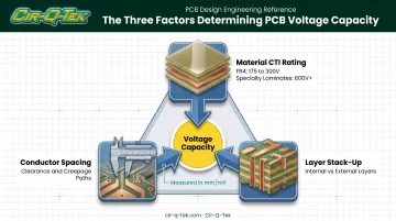
Voltage capacity comes down to three factors:
- Material CTI rating — how resistant the laminate surface is to tracking failure
- Conductor spacing — both clearance (through air) and creepage (along the surface)
- Layer stack-up — internal layers follow different spacing rules than external ones
Standard FR4 typically falls in the CTI 175–300V range, while specialty laminates built for kV-range switching gear carry CTI ratings above 600V. A board's real voltage ceiling comes from how these material properties combine with layout spacing decisions, not from a single spec sheet number.
The same creepage and clearance math applies to rigid, flex, and rigid-flex boards. Flex designs need extra care at bend zones, where creepage paths can shift under cycling; rigid-flex often needs more margin at the transition zone. Material and spacing choices adjust by construction type, but the underlying rules do not.
Demand for high-voltage PCB expertise is rising with EVs, renewables, and industrial power electronics. The EV-specific PCB market alone was valued at $1.7 billion in 2024 and is projected to reach $4.4 billion by 2035, about an 8.5% CAGR.
Creepage, Clearance, and Safety Standards
Clearance vs. Creepage
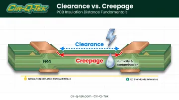
Clearance is the shortest distance through air between two conductors. Creepage is the shortest path across an insulating surface between them. Both need separate calculations because they fail under different conditions.
Clearance dominates in clean, dry environments where air is the primary insulator. Creepage becomes the limiting factor once humidity, dust, or pollution enter the picture. A damp or contaminated surface can carry a tracking current well below what clean air would allow.
Corona is a related failure mode. When electric field strength around a conductor exceeds air's local breakdown threshold, the air ionizes. That produces a faint hissing sound, generates ozone, and bleeds power as leakage current.
Risk climbs at altitude and in low-pressure environments, where air's insulating strength drops sharply. Sharp copper edges make it worse by concentrating field lines at a point.
IPC-2221B: The Primary Spacing Standard
IPC-2221B Table 6-1 is the reference most fabricators and designers use to set minimum spacing. It breaks requirements down by installation category — internal layers, uncoated external at sea level, uncoated external above 3,050 meters, polymer-coated, and conformal-coated — because each environment tolerates different risk levels.
Selected ranges from Table 6-1 for internal conductors (column B1) — not the full table:
| Peak AC or DC Voltage | Minimum Spacing (B1, internal) |
|---|---|
| 0-15V | 0.05 mm |
| 51-100V | 0.10 mm |
| 101-150V | 0.20 mm |
| 251-300V | 0.20 mm |
| 301-500V | 0.25 mm |
Above 500V, spacing follows a per-volt adder instead of a fixed table value:
Spacing = 500V row value + (working voltage − 500V) × column adder
For internal conductors, Altium's worked example at 580V calculates to 0.25mm + (80V × 0.0025mm) = 0.45mm. Get the installation category wrong, and every downstream spacing calculation is wrong too.
Supporting Standards, Materials, and Layout Tactics
IPC-2221 doesn't work alone. Depending on the application, designers also reference:
- IEC 60664-1 — clearance, creepage, and solid insulation coordination up to 1,000V AC or 1,500V DC, with altitude adjustments
- IEC 62368-1 — safety requirements for AV/ICT equipment (successor to IEC 60950-1)
- UL 796 — the core safety standard for printed wiring boards
Material insulation adequacy for creepage calculations is graded by Comparative Tracking Index category, or PLC:
| PLC Category | CTI Range |
|---|---|
| PLC 0 | ≥600V |
| PLC 1 | 400-599V |
| PLC 2 | 250-399V |
| PLC 3 | 175-249V |
| PLC 4 | 100-174V |
| PLC 5 | <100V |
Two layout tactics reclaim board space without relaxing those ratings:
- Non-plated slots or cutouts between conductors lengthen the creepage path without adding board area—current must travel around the slot instead of straight across
- Rounded trace and pad corners cut field concentration at sharp points and lower corona risk at the same voltage
Choosing the Right Materials for High-Voltage PCBs
Substrate Options at a Glance
No single laminate works for every high-voltage project. Cost and performance trade off against each other:
| Material Type | Typical CTI / PLC | Best Fit |
|---|---|---|
| Standard FR4 | PLC 3, ~175-250V | Moderate HV, cost-sensitive designs |
| Phenolic-cured FR4 (e.g., Ventec VT-47) | PLC 3, 175-250V | CAF-resistant builds needing heavy copper |
| E-glass epoxy (e.g., Isola IS400) | PLC 3, 175-249V | CAF-resistant multilayer boards |
| Ceramic-filled PTFE (e.g., Rogers CLTE-MW) | PLC 0, ≥600V | kV-range switching and RF power |
These are product-specific ratings, not family-wide guarantees. Always check the actual datasheet rather than assuming every FR4 or PTFE laminate performs the same.
Resin Content and Glass Weave
Conductive Anodic Filamentation (CAF) is a slow-growing failure mode where conductive filaments form along glass fibers under voltage and moisture. Higher resin content combined with finer glass weaves reduces the exposed fiber path available for filament growth.
Isola's 185HR prepreg data shows resin content varying by weave style: roughly 67-72% for 1080 style, 60% for 2113, and 57% for 2116. Finer weaves paired with higher resin content generally support better long-term reliability in humid or contaminated environments, though CAF resistance ultimately depends on the full laminate system, not resin percentage alone.
Copper Weight and Surface Finish
High-voltage boards that also carry high current need heavier copper. Some phenolic-cured laminates support up to 12 oz copper. Once current exceeds roughly 10A, 1–3 oz is the common industry range.
Surface finish affects solderability and long-term reliability under voltage and environmental stress. Choose among ENIG, immersion silver, immersion tin, or HASL based on the board’s service environment, not assembly process alone.
What's the Best Material for High-Voltage Applications?
There isn't one. Ceramic-filled or HVPF-type laminates suit kV-range designs where CTI ratings above 600V are non-negotiable. High-CTI FR4 variants often suffice for boards operating in the low-to-mid hundreds of volts. Voltage range, environment, and budget drive the choice. Make that call with an experienced fabricator rather than guessing from a datasheet alone.
Cir-Q-Tek’s fabrication network handles specialty substrates and mixed-technology lamination beyond standard FR4, with domestic support for matching material options to your voltage class and environment.
Best Practices for High-Voltage PCB Layout
Design Beyond the Code Minimum
Code minimums in IPC-2221 assume a defined environment. Real-world boards see condensation, dust, and contamination the base tables don't fully account for. Two habits reduce risk:
- Widen spacing beyond minimum values in zones prone to moisture or debris buildup
- Physically and electrically separate high-voltage and low-voltage circuit zones, rather than routing them side by side
Conformal Coatings Add a Margin of Safety
Acrylic, urethane, and silicone conformal coatings protect against moisture and dust, which matters most in automotive, industrial, and outdoor equipment.
IEC 60664-3 permits reduced clearance and creepage distances only when a coating, potting, or molding system has been formally validated under one of its two protection methods. Coating alone doesn't automatically provide extra spacing margin unless it's been qualified that way.
Automate What You Can
Manual spacing checks don't scale on dense HV boards. Two practical habits:
- Use EDA tool DRC engines with dedicated "HV" net classes so spacing violations get flagged automatically during layout, not after fabrication
- Label high-voltage zones clearly on silkscreen and documentation so assembly, test, and inspection teams know where extra caution applies
Common Applications of High-Voltage PCBs
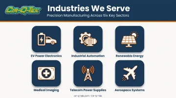
High-voltage PCB design shows up across a wider range of industries than most people expect:
- EV power electronics — inverters, onboard chargers, and battery management systems
- Industrial process control and automation — motor drives, power supplies, and switching equipment
- Renewable energy and power conversion — solar inverters and grid-tie equipment
- Medical imaging and therapeutic devices — higher-voltage pulse systems for imaging and treatment
- Telecom power supplies — equipment operating outside standard low-voltage ranges
- Aerospace and high-altitude systems — avionics, cabin electronics, and low-pressure industrial sites
Several of these applications also leave sea-level conditions behind, and that changes the clearance rules.
High-Altitude and Low-Pressure Environments
Low-pressure air loses insulating strength as altitude rises. Voltages that are safe at sea level can arc in aircraft cabins, spacecraft, or high-elevation industrial sites. Spacing that passes on the bench may not hold at 30,000+ feet.
Designs for these environments need extra margin from day one, not as a late add-on.
Medical, automotive, industrial, and telecom work dominates this list, so the manufacturing partner has to match that regulatory reality. Certifications matter as much as the layout itself.
Partnering with the Right PCB Manufacturer for High-Voltage Designs
Certifications Aren't Just Paperwork
Compliance-heavy HV projects need a fabricator whose quality system matches the target industry. Cir-Q-Tek holds ISO 9001 for general quality management, ISO 13485 for medical device manufacturing, and IATF 16949 for automotive requirements.
Those certifications match the quality systems medical, automotive, and industrial HV programs usually require, so the paperwork trail regulators ask for is built into the process instead of added later.
Prototyping Before You Commit to Production
Creepage and clearance layouts look correct on screen and still need physical validation. Cir-Q-Tek's quick-turn prototype service, 3 days to build, 2 days to ship, gives engineering teams a fast way to catch spacing or material issues before committing to a full production run.
Fabrication Capabilities That Matter for HV Boards
A few capabilities are worth confirming with any HV fabrication partner:
- Multilayer construction up to 40 layers, useful for separating HV and LV planes internally
- Heavy copper processing for boards combining high current with high voltage
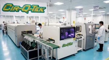
- SMT lines with inline AOI and X-ray inspection to catch assembly defects before they become field failures
- CAD/CAM support for stack-up planning and material selection guidance
Cir-Q-Tek offers all four, plus a secondary quality inspection stage at its Pennsylvania facility before boards ship. On a prototype-to-production path, that mix of certification, fast iteration, and layered inspection makes spacing and material mistakes harder to miss.
If you're scoping a high-voltage board, requesting a quote with your Gerber package and BOM is the fastest way to get application-specific guidance on materials, copper weight, and stack-up for your voltage class.
Frequently Asked Questions
What is a high-voltage PCB?
A high-voltage PCB is designed to safely carry voltages typically above 100V DC or 30V RMS AC. It uses spacing, materials, and insulation choices that go beyond standard board design. The exact threshold shifts depending on industry and applicable safety standard.
How many volts can a PCB handle?
There's no fixed number. Voltage capacity depends on material CTI rating, conductor spacing, and layer stack-up. With the right design choices, a board can safely handle anywhere from a few hundred volts to several kilovolts.
What is the best PCB material for high-voltage applications?
It depends on the voltage range. High-CTI FR4 variants often work for moderate high-voltage needs, while HVPF or ceramic-filled laminates suit kV-range designs.
What are the three types of PCBs?
The three primary types are rigid, flexible, and rigid-flex PCBs. High-voltage design principles apply to all three, with spacing and material choices adjusted for each construction type.
What is the difference between clearance and creepage?
Clearance is the shortest through-air distance between conductors, while creepage is the shortest path along an insulating surface. Both must be checked separately since each fails under different environmental conditions.
What standards govern high-voltage PCB design?
IPC-2221 is the primary spacing standard, supported by IEC 60664-1 for insulation coordination, IEC 62368-1 for IT and AV equipment safety, and UL 796 for printed wiring board safety.