Introduction
PCB manufacturing is the multi-stage process of turning a digital circuit design into a physical, functional printed circuit board. Imaging, etching, drilling, plating, and finishing each transform a flat sheet of copper-clad laminate into working hardware.
This guide is written for engineers, product developers, and procurement teams working in medical, automotive, telecom, and industrial electronics. If you need fabrication at an operational level—not just a conceptual overview—start here.
One persistent snag: teams use "PCB manufacturing" interchangeably with PCB design or PCB assembly. That mix-up drives miscommunication between OEMs and fabricators and is often why projects slip.
Below, we cover how the process works step by step, what drives quality, cost, and lead time, and when an experienced manufacturing partner is worth bringing in.
Key Takeaways
- Gerber or ODB++ files become bare boards via imaging, etching, drilling, plating, and finishing.
- Medical, automotive, telecom, and industrial sectors rely on this process for performance and compliance.
- Multilayer, HDI, and rigid-flex boards need extra lamination and alignment versus simpler designs.
- Material, layer count, surface finish, and order volume drive most cost and timeline variation.
- An ISO-certified, one-stop partner reduces design-for-manufacturability errors and quality failures.
What Is the PCB Manufacturing Process (and Why It Matters)
PCB manufacturing is the fabrication of a bare, non-conductive board with etched conductive copper traces, vias, and finishes built from a verified digital design file. The goal is a physical board that carries electrical signals reliably between mounted components, with zero shorts, opens, or hidden defects.
Fabrication is not assembly. Fabrication builds the bare board itself: copper layers, vias, solder mask, and finish. Assembly (PCBA) comes afterward, mounting and soldering components onto that finished board. Confusing the two is one of the most common breakdowns between OEMs and their manufacturing partners.
That distinction matters because many quality failures start at the bare-board stage, long before components are placed. The global PCB market was valued at $74.12 billion in 2025 and is projected to reach $129.65 billion by 2034, growing at a 6.65% CAGR, according to Fortune Business Insights. Bare-board quality sits at the center of nearly every electronics category in use today.
Without disciplined process control, boards fail in the field—often only after install in a vehicle or hospital device. Critical controls include:
- DFM checks before fabrication starts
- Automated optical inspection (AOI)
- Electrical testing for shorts and opens
Common hidden defects include shorts, delamination, and trace flaws that are invisible until power-up. This guide walks through each major fabrication step, the controls that catch those defects, and what OEMs should verify with their manufacturing partner.
How PCBs Are Made: The Complete Step-by-Step Manufacturing Process
Design files go in; CAM processing and panelization prepare the data; then copper patterning, etching, drilling, and plating build the physical layers. Multiple inspection checkpoints run throughout, not just at the end.
A flat sheet of copper-clad laminate becomes a fully patterned, plated, and finished circuit board ready for assembly. Construction is largely identical for the first layer regardless of final board type. Complexity rises as you add layers for multilayer, HDI, or rigid-flex designs.
Fabricators rely on computer-guided machinery (CAM software, laser direct imaging, computer-controlled drills) to hold precision at nearly every stage. At line widths measured in thousandths of an inch, human error simply isn't tolerable.
NCAB Group's multilayer PCB production guide documents 33 discrete production steps for a standard multilayer board. That count varies by shop and board type, but it shows how granular the process becomes once you separate imaging, etching, plating, and inspection.
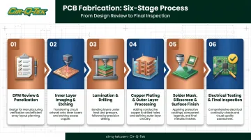
Step 1: Pre-Production Engineering and DFM Review
Before anything gets built, the fabricator runs a Design for Manufacturability (DFM) check on the submitted Gerber or ODB++ files. This verifies:
- Trace width and spacing against the shop's capabilities
- Hole sizes and aspect ratios
- Layer stack-up consistency
Once the design passes DFM, the fabricator panelizes multiple board copies onto one large production panel to maximize material usage and run efficiency.
Step 2: Inner Layer Imaging and Etching
Operators apply photoresist to the copper-clad laminate, then image it (commonly with laser direct imaging, or LDI) to create the circuit pattern. LDI has largely replaced older film-based phototool methods because it eliminates distortion, shrinkage, and positional errors during imaging.
After imaging, the panel is etched. Chemical etching removes unwanted copper and reveals the designed traces on the inner layers.
Step 3: Lamination and Drilling
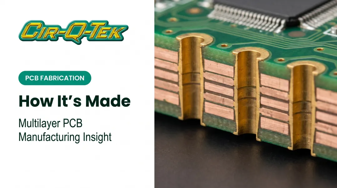
For multilayer boards, fabricators stack inner layers, prepreg, and copper foil, then bond them under heat and pressure in a laminating press. That cycle fuses the individual layers into a single rigid structure.
Once laminated, computer-guided drills create the holes needed for standard vias and component leads. For finer features like blind or buried vias, laser drilling handles the microvia work. Some fabricators can drill holes down to roughly 0.0039 inches for HDI applications.
Step 4: Copper Plating and Outer Layer Processing
Electroless copper deposition coats the drilled holes and outer layers, followed by electrolytic plating. This builds the conductive pathways that connect one layer to another through the board.
After plating, the outer layers go through their own imaging and etching cycle to define the final outer circuit pattern. The sequence mirrors the inner-layer process from Step 2, but on the completed, drilled panel.
Step 5: Solder Mask, Silkscreen, and Surface Finish
The shop applies a liquid photo-imageable solder mask across the board to protect copper and prevent solder bridging during later assembly. Technicians then print silkscreen legends for component reference markings.
Finally, the board receives a surface finish to prevent oxidation and keep the copper solderable. Common options include:
- HASL: cost-effective, widely used for general commercial boards
- ENIG: flat surface, good for fine-pitch and BGA components
- OSP: flat and low-cost, but shorter shelf life
- Immersion silver or tin: flat surfaces with handling-sensitivity trade-offs
Step 6: Electrical Testing, Routing, and Final Inspection
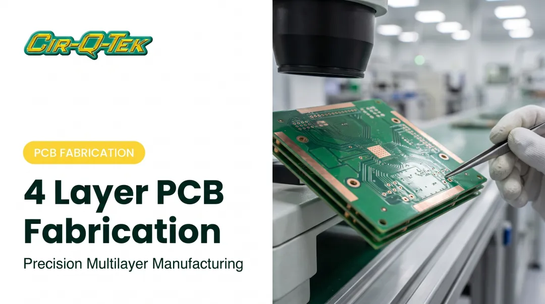
Bare boards undergo electrical testing to catch shorts and opens before they ever leave the factory. Routing or V-scoring then separates boards from the panel into individual units.
A final visual and dimensional inspection follows before packaging and shipment, the last checkpoint before boards head to assembly.
Where PCB Manufacturing Is Applied Across Industries
Fabricated PCBs show up everywhere modern electronics operate:
- Medical devices requiring traceable, high-reliability boards
- Automotive control modules under thermal and vibration stress
- Telecom infrastructure equipment
- Industrial process control systems
- Consumer and commercial electronics
Fabrication isn't a one-time event. It recurs across a product's lifecycle: prototyping, design validation, pilot runs, and full-scale production. Each stage has different volume needs and turnaround expectations, and a design revision, new SKU, or volume ramp-up can trigger the process again.
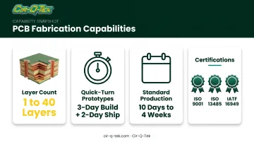
That industry spread is why certification breadth matters. Cir-Q-Tek covers commercial, medical, and automotive requirements under one roof through ISO 9001, ISO 13485, and IATF 16949-certified facilities.
PCB capabilities run from single-sided boards through 40-layer multilayers, with quick-turn prototypes built in 3 days and shipped in 2, and standard production delivered in 10 days to 4 weeks.
Key Factors That Affect PCB Manufacturing Quality, Timeline, and Cost
Several variables determine what a board will cost and how long it will take to build:
- Materials and copper weight — Substrate type (FR-4, high-Tg, Rogers), copper thickness, and layer count directly affect signal performance and unit cost.
- Process conditions — Etching chemistry, lamination temperature and pressure, and plating bath control determine trace precision and interlayer bond strength.
- Equipment capabilities — Laser direct imaging, precision drilling, and AOI/X-ray inspection set the tolerances a shop can hold on trace width, hole size, and layer registration.
- Volume and turnaround — Prototype runs measured in days differ sharply from production runs measured in weeks, affecting panel utilization and per-unit pricing.
- Compliance requirements — Medical (ISO 13485) and automotive (IATF 16949) applications require additional documentation and traceability, adding time and cost versus standard commercial boards.
- Design complexity — Multilayer, HDI, and rigid-flex designs require extra lamination and alignment steps that increase both lead time and cost.
According to PCD&F's cost analysis, base laminate material typically runs around 20% of total bare-board fabrication cost, with layer count and via technology as additional major drivers.
Getting an itemized quote against your actual design files—not a generic per-board estimate—is the only reliable way to pin down real cost.
Common Mistakes, Misconceptions, and When to Partner with an Expert Manufacturer
A few misconceptions cause more delays and re-spins than almost anything else in this industry.
Manufacturing and assembly aren't the same thing. Fabrication builds the bare board. Assembly populates it with components. Teams that treat these as interchangeable often submit the wrong files to the wrong vendor, or set unrealistic expectations for turnaround.
A completed CAD design isn't automatically manufacturable. Plenty of teams assume their design file is ready to go straight to production. A proper DFM review catches trace, spacing, or hole errors before they turn into a costly re-spin weeks later.
Passing inspection isn't the same as long-term reliability. AOI and electrical testing catch manufacturing defects such as shorts, opens, and plating voids. They don't validate long-term thermal performance or design-level reliability issues that only surface after months in the field.
Attempting in-house or single-vendor fabrication without ISO-certified processes, multi-stage inspection, or coordinated offshore-domestic project management often produces inconsistent quality and missed deadlines. That risk is highest in regulated industries.
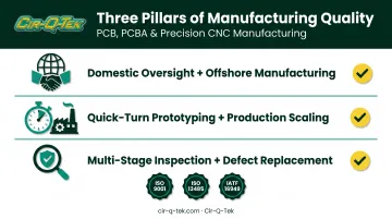
For medical, automotive, or high-complexity boards, a one-stop partner certified to ISO 9001, ISO 13485, and IATF 16949 reduces exposure substantially. Look for:
- Domestic project oversight paired with offshore manufacturing capacity
- Quick-turn prototyping alongside production scaling
- Multi-stage inspection and a clear defect-replacement policy
Cir-Q-Tek, for example, combines Pennsylvania-based project management with Shenzhen manufacturing pricing, plus quick-turn prototypes and no-cost replacement for non-compliant parts.
Knowing each fabrication step helps teams specify requirements clearly and catch DFM errors before they become the most expensive delays.
Frequently Asked Questions
How much does it cost to get a PCB manufactured?
Cost depends on layer count, board size, material, surface finish, and order volume. Prototype quantities cost more per unit than production runs. Request an itemized quote for accurate pricing.
What's the difference between PCB fabrication and PCB assembly?
Fabrication builds the bare board: copper traces, layers, and finishes. Assembly (PCBA) involves mounting and soldering components onto that finished board.
How many layers can a PCB have?
Boards range from single or double-sided up to 40-layer multilayer designs for high-complexity applications. Layer count is driven by circuit density and signal requirements.
What file format do I need to submit for PCB manufacturing?
Gerber or ODB++ files are standard for fabrication, along with a Bill of Materials (BOM) if assembly is also required. Some fabricators also accept IPC-2581.
How do I choose the right surface finish for my PCB?
Match the finish to cost, shelf life, and application needs. HASL works well for general use, while ENIG suits fine-pitch or high-reliability boards such as those used in medical and automotive applications.
What is the fastest PCB manufacturing turnaround time available?
Quick-turn prototyping can deliver boards in as little as 3 days to build plus 2 days to ship. Standard production runs typically take 10 days to 4 weeks depending on complexity and volume.