
That's where 8 layers come in. Signal integrity problems, EMI leakage, and power distribution headaches often trace back to a stackup that simply doesn't have enough reference planes or routing channels. Adding two more layers changes the math.
This guide covers stackup configurations, material choices, thickness ranges, design best practices, and how to pick a manufacturing partner that won't leave you guessing about what's actually inside your board.
Key Takeaways
- Dedicated ground cages and power-ground plane pairs fix signal integrity issues 6-layer boards can't solve
- Five common configurations exist, each trading off signal layers against reference planes and EMI suppression
- Expect roughly a 30-35% cost increase over 6-layer boards, driven by the second lamination cycle
- Symmetric, balanced copper distribution during layout prevents warpage during fabrication
- Confirm core/prepreg data and impedance tolerances with your fabricator, not a generic diagram
What Is an 8-Layer PCB Stackup?
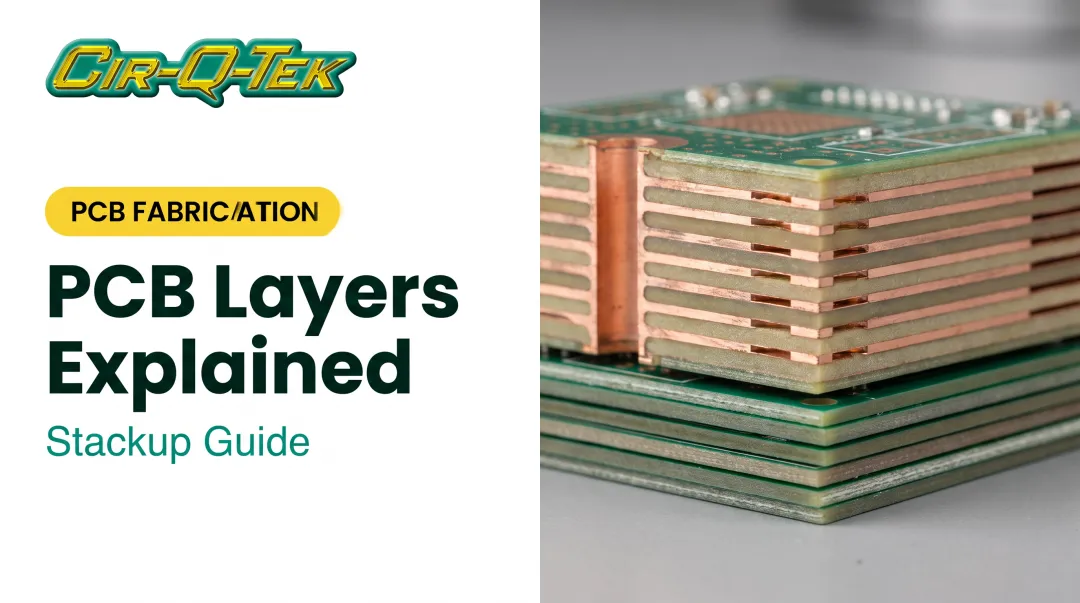
An 8-layer PCB stackup is the sequential arrangement of eight copper layers and intervening dielectrics laminated into one rigid board. Layer order and symmetry determine impedance control, EMI behavior, and whether the board warps during manufacturing.
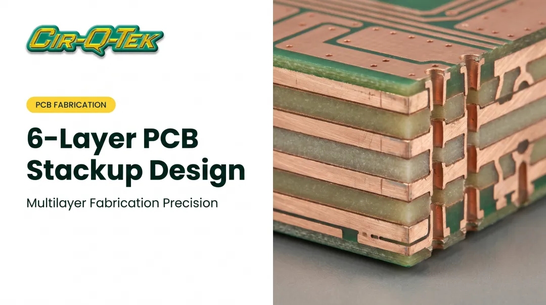
Compared to a 6-layer board, going to 8 layers typically adds:
- Dedicated ground cage for shorter signal return paths
- Real power-ground plane pairs instead of sharing one pair across multiple functions
- More routing channels for dense BGA and mixed-signal designs
The trade-off: two lamination cycles instead of one. That means more press time, an extra drilling pass, and a longer lead time than a single-cycle 6-layer build.
Where 8-Layer Boards Show Up
Motherboards, telecom equipment, FPGA/SoC boards, and regulated medical and automotive electronics all lean on 8 layers when routing density or reference-plane integrity becomes non-negotiable.
Broader industry data backs the trend toward higher layer counts: IPC's technology trends report found HDI usage climbing from 37.5% to just over 49% over five years, based on data from 60 PCB manufacturers. That's not an 8-layer-specific figure, but it tracks with the same underlying pressure: more density, fewer layers to spare.
Standard 8-Layer Stackup Configurations
There's no single "correct" 8-layer order. Fabricators typically offer several proven arrangements, each suited to a different priority.
Balanced Power Integrity Stackup
This configuration places power and ground plane pairs so that every signal layer sits adjacent to a reference plane. A typical order runs:
Signal / GND / Signal / PWR / GND / Signal / PWR / Signal
Choose this when consistent impedance control across all signal layers matters more than raw routing capacity.
EMI-Optimized "Ground Cage" Stackup
Add a third ground layer to shorten return paths further and wrap signal layers in ground on both sides where possible. A typical order runs:
Signal / GND / Signal / GND / PWR / GND / Signal / GND
This setup suits EMI-sensitive work—RF-adjacent digital circuits or noisy automotive environments.
Symmetric Stripline Stackup
Two full plane pairs sandwich the inner signal layers, isolating them as true striplines while keeping the physical buildup mechanically symmetric. A typical order runs:
Signal / GND / Signal / PWR / PWR / Signal / GND / Signal
You get dedicated power distribution layers plus tightly controlled impedance on the inner signals.
Maximum Signal Layer Stackup
Here you sacrifice reference planes for routing room. A typical order runs:
Signal / Signal / GND / Signal / Signal / PWR / Signal / Signal

This only makes sense when:
- Impedance requirements are genuinely relaxed
- The board is routing-density constrained, not signal-integrity constrained
- High-speed serial links still sit next to a ground reference
Whichever configuration you choose, the final result depends heavily on prepreg and core selection. Dielectric thickness determines how tightly signals couple to their reference planes, so the stackup diagram is only half the story.
Materials, Thickness, and Dimensions
Copper weight and dielectric choice shape both electrical performance and final board thickness.
Copper foil options:
- 0.5oz outer layers are common for fine-pitch, low-current designs
- 1oz inner/outer copper handles moderate current and is the most widely used default
- 2oz and above for boards carrying meaningful current on power layers
Dielectric materials:
- FR-4 (standard or high-Tg) for most commercial and industrial applications
- Rogers or PTFE-based laminates for RF and high-frequency signal paths, where lower loss tangent matters
Common FR-4 prepregs such as 2116 and 7628 glass styles run dielectric constants around 4.45-4.74, with FR-4 cores near Dk 4.6.
Finished thickness for 8-layer boards commonly falls in the 1.0mm to 2.5mm range. Board dimensions and panelization depend on component density and the target enclosure, so confirm final numbers with your fabricator rather than a spec-sheet estimate alone.

8-Layer vs. 6-Layer PCB: Making the Right Choice
| Factor | 6-Layer | 8-Layer |
|---|---|---|
| Usable signal layers | Typically ~4 | 4-6, depending on configuration |
| Reference planes | Usually one plane pair | Often two plane pairs |
| Cost impact | Baseline | ~30-35% higher |
| Lead time | Single lamination cycle | Two lamination cycles + extra drilling |
The routing gap isn't always dramatic. A well-optimized 6-layer board can sometimes match a poorly planned 8-layer one. What really separates the two is reference-plane integrity. Two plane pairs instead of one make impedance and EMI behavior far more predictable.
Rule of thumb: if your 6-layer design keeps failing DRC, or you can't find room for a second reference plane without gutting your routing channels, 8 layers is the more predictable path forward. Fighting a 6-layer stackup past its limits usually costs more in respin time than the extra layers would have cost upfront.

Design Best Practices for 8-Layer Stackups
Getting the stackup right on paper doesn't guarantee a clean board. A few habits make the difference:
- Keep high-speed signals adjacent to continuous reference planes. This controls impedance and cuts crosstalk between neighboring traces.
- Separate analog and digital sections physically so switching noise from digital circuits doesn't couple into sensitive analog paths.
- Maintain symmetric, balanced copper distribution across the stackup. Uneven copper density between layers is a common cause of warpage during lamination.
- Validate your stackup with impedance calculation tools before finalizing layout, not after.
Avoid plane splits and cutouts wherever possible. Every hole in a reference plane increases loop area for return currents, which directly increases radiated noise and impedance discontinuities. If a signal must cross a plane split, keep it over the correct reference region on both sides.
Choosing the Right Manufacturing Partner for Your 8-Layer PCB
A stackup diagram on a website is a starting point, not a guarantee. What actually determines whether your board hits target impedance is the real core and prepreg thickness, resin content, and copper weight your fabricator uses on the production line, not the generic example in a blog post.
That's worth confirming directly with any manufacturer before you commit to a design.
Turnkey capability matters here too. Handling fabrication and assembly under one roof removes a handoff point where miscommunication about stackup tolerances tends to creep in.
Cir-Q-Tek fabricates PCBs up to 40-layer multilayers with capabilities that support complex 8-layer builds:
- Laser direct imaging that avoids distortion and positional errors from traditional photo-imaging
- Blind and buried vias, with laser-drilled holes down to 0.0039 inches
- Fine line/spacing to 0.0025"/0.0025"
- Quick-turn prototypes on a 3-day build, 2-day ship schedule
- ISO 9001, IATF 16949, and ISO 13485 certification for automotive and medical applications

Cir-Q-Tek's dual office model, headquartered in Bristol, Pennsylvania with a Shenzhen, China operation, pairs domestic project management with offshore manufacturing economics. Bilingual staff in Shenzhen handle communication directly with production, which matters more on complex multilayer builds where a misread stackup note can mean a respin.
Before comparing quotes, confirm:
- Impedance tolerance the fabricator will actually hold, not just target
- Available HDI upgrade paths, including blind/buried via structures
- Defect replacement policy for non-compliant parts (Cir-Q-Tek replaces non-compliant parts at no additional cost)
Frequently Asked Questions
What are PCB layers?
PCB layers are the alternating conductive copper and insulating dielectric layers laminated together into one board. They route signals, power, and ground throughout the circuit.
What is a 6-layer PCB?
A 6-layer PCB typically has around four signal layers plus one ground-power plane pair. It offers less routing room and fewer reference planes than an 8-layer board, making it suitable for moderate-density designs.
How much more does an 8-layer PCB cost compared to a 6-layer PCB?
There's no fixed markup. Estimates put the increase around 30-35%, but actual cost scales with lamination cycles, board thickness, copper weight, and order quantity.
Can an 8-layer PCB support blind and buried vias?
Standard 8-layer builds use through-hole vias only. HDI structures with laser-drilled blind and buried vias can be added when a design needs them.
What industries commonly use 8-layer PCBs?
Telecom, automotive, medical devices, and industrial control systems commonly require 8-layer boards for the routing density and power integrity these applications demand.
How do I know if my design needs 8 layers instead of 6?
Watch for DRC failures, insufficient reference planes for your signal layers, or dense BGA and mixed-signal routing that won't fit cleanly on 6 layers. Any of these means it's time to move up.