
As designs pack more into less space — fine-pitch BGAs, 01005 components, QFN packages with hidden leads — visual inspection alone can't keep up. For OEMs in medical, automotive, and industrial sectors, PCBA testing isn't a nice-to-have. It's the line between a reliable product and a costly field failure.
This guide breaks down what PCBA testing actually involves, the major testing methods available, how to pick the right one for your project, and how a manufacturing partner like Cir-Q-Tek builds testing into every build from prototype to production.
Key Takeaways
- PCBA testing confirms assembled boards meet spec and catches defects while they are still cheap to fix
- No single method catches everything — reliable programs layer AOI, ICT, X-ray, and functional testing
- Testing strategy should shift as a product moves from prototype to full production
- An ISO-certified manufacturing partner can own test setup so you avoid building that infrastructure in-house
What Is PCBA Testing and Why Does It Matter?
PCBA testing is the process of verifying an assembled circuit board for defects, functionality, and reliability before it ships. It covers everything from checking that components are correctly placed to confirming the board performs as designed under real conditions.
Here's a distinction worth nailing down: a PCB (printed circuit board) is the bare, unpopulated substrate: just copper traces and layers, no components. A PCBA (printed circuit board assembly) is that same board once it's been populated with resistors, capacitors, ICs, and connectors. You test the PCBA because that's the version that actually has to work.
The later a defect is caught, the more it costs to fix. A board with a bad solder joint is far cheaper to rework on the line than after it ships, installs, and fails in the field. Diagnosis, logistics, and warranty exposure all pile onto that later repair cost.
That's exactly why regulated industries build testing into their quality systems rather than treating it as optional:
- Medical device manufacturers operate under ISO 13485, which requires a documented, traceable quality management system tied to the finished device
- Automotive suppliers work under IATF 16949, where customer-specific requirements often demand control-plan-linked measurement, test, and traceability records
Neither standard prescribes one universal test sequence, but both require a validated, documented testing strategy appropriate to the product's risk level.
Common PCBA Testing Methods
No single test catches every defect type. The most reliable programs layer multiple methods, each covering a different failure class. Here's what that looks like in practice.
Automated Optical Inspection (AOI)
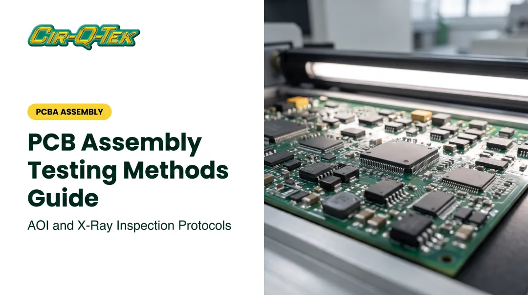
AOI uses cameras and programmed criteria to scan every board for visible defects: missing components, misaligned parts, solder bridges, tombstoning, and polarity errors.
Why it's the workhorse of most lines:
- Requires no dedicated fixture
- Screens every board, not just a sample
- Fast enough to run inline without slowing production
Its limitation? AOI can only see what the camera can see. Hidden solder joints under a BGA are invisible to it — that's a job for X-ray, covered below.

In-Circuit Testing (ICT)
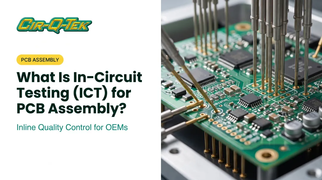
ICT uses a "bed of nails" fixture (hundreds of spring-loaded pins that make contact with test points on the board) to verify component values, shorts, opens, and net-level connections.
ICT suits designs that are:
- Stable (not going through frequent revisions)
- High-volume (justifying the fixture investment)
- Accessible (enough exposed test points for pin contact)
Dense, fine-pitch boards with BGAs reduce ICT's coverage since there's less physical access to probe. In those cases, ICT typically works alongside AOI or X-ray rather than standing alone.
Flying Probe Testing
Flying probe testing does a similar job to ICT — checking component values and connections — but uses software-controlled, moving probes instead of a fixed fixture.
This makes it the go-to for:
- Prototypes and NPI (new product introduction) builds
- Low-to-medium volume runs
- Designs still likely to change
It's slower than ICT per board, so it doesn't scale well to high volume, but you skip the fixture cost and lead time entirely.
X-Ray Inspection (AXI)
BGA, QFN, and other leadless packages hide their solder joints underneath the component body. No camera can see them. X-ray inspection solves this by imaging straight through the package to reveal voiding, insufficient solder, bridging, and the notorious "head-in-pillow" defect.
Cir-Q-Tek runs inline AOI and X-ray inspection on every SMT line, which matters directly for boards using 01005 components, 0.2mm BGA spacing, QFN, and CSP packages — exactly the package types where hidden joints are a real risk.
Functional Testing (FCT)
Functional testing powers the board up and runs it through its actual intended function (signal outputs, communication interfaces, sensor responses) under conditions close to the real application.
FCT doesn't replace component-level tests like ICT or AOI. It complements them:
- ICT confirms components are the right value and correctly connected
- AOI confirms visible placement and solder quality
- FCT confirms the whole board actually does its job
A board can sail through ICT and still fail FCT if there's a design issue or an interaction problem that only shows up when everything's running together.

Choosing the Right Testing Method for Your Project
Method selection comes down to three variables: production volume, board complexity, and compliance requirements. Here's how that typically plays out across a product's lifecycle.
Prototype / NPI stage
- AOI plus functional testing, or flying probe for electrical checks
- Fixture investment isn't justified yet. You don't know if the design will change
Low-to-mid volume
- Flying probe or simple fixtures
- Evaluate fixture ROI against total expected volume before committing
High-volume production
- ICT with a dedicated bed-of-nails fixture for speed and coverage
- AOI as a first-pass screen on every board
- Functional testing for final system-level validation
Highly complex boards (dense BGAs, mixed fine-pitch and through-hole) usually need a multi-method approach regardless of volume, since no single test covers every failure mode on a board this dense.
| Method | Defect Type Caught | Fixture Required | Ideal Volume |
|---|---|---|---|
| AOI | Placement, solder bridges, missing parts | No | Any |
| Flying Probe | Component values, opens/shorts | No | Prototype–low |
| ICT | Component values, net faults | Yes (bed of nails) | High, stable design |
| X-Ray (AXI) | Hidden BGA/QFN solder joints | No | Any, especially complex packages |
| FCT | Whole-board functional behavior | Sometimes (test jig) | Any |

Common Mistakes That Compromise PCBA Quality
Even solid components and a good layout can end up untestable when test access is ignored early:
- No accessible test points — if probe access wasn't designed in from the start, retrofitting it later is expensive, sometimes impossible without a board redesign
- Relying on functional testing alone — FCT tells you the board failed, not why; without ICT or AOI data, you're stuck guessing which component caused it
- Treating test planning as an afterthought — bringing test engineers in after layout is locked means probe access and fixture design get bolted on late and schedules slip
The fix for all three is the same: involve testing considerations during design, not after the first prototype run fails.
How Cir-Q-Tek Builds Reliable Testing Into Every PCBA Build
Cir-Q-Tek's SMT lines run inline AOI and X-ray inspection on every board as part of the standard assembly process, not an optional add-on. That matters for the dense boards OEMs design today.
In practice, that standard covers:
- 01005 components, BGAs with 0.2mm spacing, QFN, and CSP packages, where hidden or fine-pitch defects are common
- Stage-by-stage material and component checks, plus finished-board verification against IPC specs and customer requirements
- A secondary quality inspection at Cir-Q-Tek's Pennsylvania facility before products are stocked or shipped
- ISO 9001:2015, ISO 13485, and IATF 16949 certifications for the documented, traceable processes medical and automotive customers need
- A defect replacement policy at no extra cost when parts don't match the fabrication information provided

Cir-Q-Tek's dual-office model pairs U.S. headquarters in Bristol, Pennsylvania, with a Shenzhen, China office. That setup supports quick-turn prototypes (3-day build, 2-day ship on PCB fabrication) and higher-volume production runs, all under the same inline inspection standard regardless of order size.
Frequently Asked Questions
What does PCBA stand for?
PCBA stands for Printed Circuit Board Assembly: a bare PCB populated with components and soldered into a functioning board.
What is PCBA vs PCB?
A PCB is the bare, unpopulated board substrate. A PCBA is that same board after components have been mounted and soldered on, making it functional.
What is the most reliable PCBA testing method?
There isn't one single "most reliable" method. A layered approach combining AOI, ICT, X-ray, and functional testing catches far more defect types than any single test run alone.
How much does PCBA testing add to manufacturing cost?
Cost varies by method and production volume. Regardless of the exact figure, testing costs are minor compared to the expense of a field failure, warranty claim, or recall.
When should I invest in a dedicated test fixture?
Fixture investment makes the most sense once your design is stable and you're not expecting frequent revisions. Below that stability threshold, flying probe testing usually offers better flexibility.
Can PCBA testing be skipped for low-volume prototypes?
Not entirely. AOI and basic functional checks are still worthwhile even at prototype stage. They catch design and assembly issues early, before those issues carry into a production run.