Introduction
Multilayer PCB manufacturing bonds three or more copper-clad layers with insulating prepreg into a single rigid board. Plated vias create electrical connections between every layer. The term comes up constantly in design reviews and RFQs, yet steps like imaging, lamination, drilling, and plating often stay a black box—even for teams that spec boards every week.
This matters most for design engineers, procurement teams, and OEMs working in medical, automotive, telecom, and industrial electronics, where board density, signal integrity, and long-term reliability aren't negotiable. A board that delaminates in the field or fails an impedance test means scrap, rework, and a program delay.
This article walks through how multilayer boards are built, which process variables change the outcome, and where the method shows up from prototype through production.
Key Takeaways
- Copper-clad cores and prepreg fuse under heat and pressure, then drill and plate into one interconnected board
- Medical monitors, automotive ECUs, and telecom base stations depend on multilayer builds for density and EMI control
- Six stages define the process: stackup planning, inner-layer imaging, lamination, drilling, plating, and finishing/testing
- Layer count, via type, and material choice drive cost, lead time, and reliability outcomes
- ISO-certified manufacturers with advanced lamination and inspection equipment cut defect rates for regulated industries
What Is Multilayer PCB Manufacturing?
Multilayer PCB manufacturing is the fabrication of a circuit board built from three or more conductive copper layers, each separated by insulating dielectric material and electrically tied together through plated vias. The layers aren't just stacked; they're pressed into a single, monolithic panel that behaves as one board, not a sandwich of separate parts.
The goal is straightforward: pack more circuitry into less space. Multilayer construction gives designers dedicated power and ground planes, tighter routing density, and better signal integrity than a single- or double-layer board can offer.
How it compares to other board types:
| Board Type | Lamination | Via Structure | Typical Use Case |
|---|---|---|---|
| Double-layer | None (no internal bonding) | Through-hole only | Simple, low-density circuits |
| Multilayer (conventional) | Single lamination cycle | Plated through-holes, blind/buried optional | Medium-to-high density boards |
| HDI | Sequential lamination | Laser microvias, stacked/staggered vias | Ultra-dense, fine-pitch designs |
Double-layer boards skip internal lamination and inner-layer via drilling entirely, since there's nothing buried inside to connect. HDI boards go a step further than standard multilayer, adding microvias and multiple sequential lamination passes for even greater density.
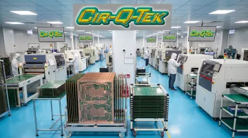
Common multilayer configurations run 4, 6, 8, and up through 40-plus layers. Layer count isn't just a function of board size; it's driven by circuit complexity and how much routing the design needs. Cir-Q-Tek's fabrication capabilities, for instance, extend from single-sided boards through 40-layer multilayers, covering that full complexity range without switching suppliers mid-program.
Why & Where Multilayer PCBs Are Used
Modern electronics need to fit far more into far less space than they did a decade ago. Smartphones, medical monitors, automotive ECUs, and telecom base stations all pack more components and interconnects into shrinking enclosures. A single- or double-layer board simply runs out of room to route them.
The broader PCB market reflects that pressure. Global PCB demand is projected to climb from $70.92 billion in 2020 to $86.17 billion by 2026, growing at a 3.3% CAGR, according to EE Times' market analysis. That growth spans the whole PCB category, but multilayer and HDI designs are taking a larger share as devices shrink and signal requirements tighten.
What multilayer construction directly solves:
- Routing density for boards with hundreds or thousands of interconnects
- Dedicated power and ground planes for EMI control
- Mechanical rigidity on larger, more complex boards
Reference planes matter more than most designers give them credit for. Place a ground or power plane close to a signal layer, with thin dielectric between them, and you cut radiation and coupling.
Nearby planes also reduce crosstalk and simplify impedance control, per PCD&F's analysis of PCB stackups. Even entry-level designs commonly use at least 4 layers for this reason, with two internal ground planes shielding outer-layer signals.
Skip multilayer construction when the design needs it, and problems show up fast: oversized boards, weaker signal integrity, higher crosstalk and EMI, and extra connectors—each one a potential failure point.
When multilayer builds show up in the product cycle:
- Prototyping and design validation before volume tooling
- Production runs for shipping products
- Stackup respins for performance or cost
Where they are used across industries:
- Medical devices that must stay reliable under regulatory scrutiny
- Automotive systems that face vibration and thermal cycling
- Telecom and 5G gear handling high-frequency signals
- Industrial process controls that run continuously
- Gaming and AV products balancing performance against cost
How Multilayer PCBs Are Made: Step-by-Step Process
The process is simple to describe and hard to execute well. Engineers image and etch individual copper-clad layers separately, stack them with prepreg, and press the stack under heat and pressure into a single panel. Drilling and plating then connect the layers electrically. Solder mask, surface finish, and testing close out the build.
Core inputs include:
- Copper foil
- FR-4 or high-frequency laminates
- Prepreg sheets
- Photoresist film
- A finalized Gerber or CAM stackup design
Lamination is the core transformation: it fuses discrete layers into one monolithic structure. Drilling and plating create the vias that tie those layers together electrically. Teams check every stage—temperature and pressure profiles during lamination, drill registration accuracy, and plating thickness—using AOI, X-ray, and cross-section inspection along the way.
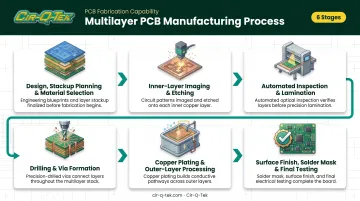
Step 1: Design, Stackup Planning & Material Selection
Before fabrication starts, engineers finalize the layer stackup—copper weight, dielectric thickness, and layer sequence. They also choose base materials such as FR-4 or high-frequency laminates based on impedance and thermal requirements. That decision locks in early because it dictates almost everything downstream: lamination cycles, drilling parameters, and final electrical performance.
Step 2: Inner-Layer Imaging & Etching
Each inner copper-clad layer receives photoresist, then exposure to the circuit pattern, development, and etching to remove unwanted copper. Precision matters most here—distortion at this stage carries through the entire stack.
Cir-Q-Tek uses laser direct imaging (LDI) for this step. LDI removes the distortion, shrinkage, and positional errors common with traditional photo-tool imaging, which is critical when fabricating boards up to 40 layers with fine line and spacing down to .0025"/.0025".
Step 3: Automated Inspection & Lamination
Each etched inner layer passes through automated optical inspection (AOI) before it ever gets near a press. AOI compares the etched circuitry against the digital design file and flags defects for an inspector to verify. Only clean layers move forward. Operators stack them with prepreg in sequence, then bond the stack under controlled heat and pressure in a press cycle that fuses everything into one panel.
Step 4: Drilling & Via Formation
Mechanical or laser drilling creates the vias that connect layers electrically, followed by desmear and deburring to clean the hole walls before plating. Blind vias (outer layer to inner layer) and buried vias (internal layers only) require extra processing steps and, often, additional lamination passes. Cir-Q-Tek's facilities support laser-drilled holes down to .0039", along with blind and buried via construction, for designs where routing density demands it.
Step 5: Copper Plating & Outer-Layer Processing
Electroless and electrolytic copper plating deposit conductive material inside the newly drilled vias and across the outer layers. Once plating is complete, the outer circuit pattern is imaged and etched to match the inner layers exactly, bringing the whole board into electrical alignment.
Step 6: Surface Finish, Solder Mask & Final Testing
Solder mask and silkscreen go on next, followed by a surface finish (ENIG, HASL, or OSP) to protect exposed copper ahead of assembly. Cir-Q-Tek offers this full range plus immersion silver and immersion tin, all RoHS-compliant. From there, the board undergoes electrical testing and final inspection, including a secondary inspection at Cir-Q-Tek's Pennsylvania facility, before it ships.
Key Factors That Affect Multilayer PCB Manufacturing
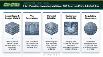
Not every multilayer board takes the same time or costs the same to build. A handful of variables determine how a design translates into lead time, cost, and defect risk.
- Layer count and copper weight: More layers and heavier copper add lamination cycles, complex drilling, and longer production time.
- Via technology: Blind, buried, and stacked vias need extra lamination cycles and precise drilling registration.
- Material selection: FR-4 covers most designs; Rogers or PTFE laminates shift dielectric performance, thermal stability, and cost for RF or high-speed work.
- Equipment capability: Laser direct imaging, inline AOI, and X-ray inspection set the ceiling for fine-pitch traces and tight BGA spacing.
- Regulatory constraints: Medical (ISO 13485) and automotive (IATF 16949) builds need tighter tolerances, full traceability, and stricter QC docs than commercial boards.
Sequential HDI builds can require anywhere from 2 to more than 4 lamination cycles, depending on blind or buried via endpoints, according to Sierra Circuits. Each added cycle compounds cost and schedule.
None of these factors work in isolation. Heavier copper on a high layer-count board with buried vias compounds every constraint at once.
A manufacturer certified to ISO 9001, ISO 13485, and IATF 16949—such as Cir-Q-Tek—keeps those variables under control on quick-turn prototypes and multi-week regulated runs alike. Submit a detailed quote request with Gerber files and a BOM so engineering can evaluate the tradeoffs before you lock the stackup.
Common Challenges, Misconceptions & When It May Not Be the Right Choice
More layers don't automatically mean better performance. Added layers increase cost and lead time, and they're only worth it when routing density or impedance control genuinely requires them. Specifying 12 layers for a board that could route cleanly on 6 just adds expense without a payoff.
Layer count alone doesn't tell the whole story, either. Two boards with the same layer count can behave completely differently depending on copper distribution and via type. Stackup design, not the number on a spec sheet, determines actual performance.
Lamination sometimes gets treated as "just pressing layers together." It isn't. Misregistration between layers or an incorrect press cycle can cause internal shorts or delamination, defects that often don't surface until the board is in the field.
Delamination cases frequently trace back to moisture accumulation at inner-layer surfaces, often rooted in poor bonding or contamination during lamination.
Multilayer construction also isn't the right call for every design. Prefer a simpler build when:
- The circuit is low-density and routes cleanly on one or two layers
- Impedance control and high-speed constraints are minimal or absent
- Cost and lead time matter more than extra routing headroom
In those cases, double-layer boards usually cost less and ship faster with no meaningful performance tradeoff. Understanding the actual process, not just specifying more layers, gets a design to the right balance of performance, manufacturability, and cost.
Frequently Asked Questions
How many layers can a multilayer PCB have?
Multilayer PCBs typically range from 4 to 20+ layers for most commercial and industrial applications. Cir-Q-Tek can fabricate up to 40 layers for complex, high-density designs.
What is the difference between blind vias and buried vias?
Blind vias connect an outer layer to an inner layer without passing through the entire board. Buried vias connect only internal layers and aren't visible from either surface.
How long does it take to manufacture a multilayer PCB?
Standard lead times depend on layer count and via complexity, typically running 10 days to 4 weeks for production orders. Quick-turn prototype services can compress that to roughly 3 days to build and 2 days to ship.
What materials are used in multilayer PCB construction?
FR-4 is the standard substrate, paired with copper foil for conductive layers and prepreg for bonding between them. High-frequency laminates, such as PTFE-based materials, are used for specialized RF or high-speed applications.
Why are multilayer PCBs more expensive than single or double-layer boards?
Every additional layer adds a lamination cycle, extra drilling steps, more plating, and another round of inspection. Those added materials, labor, and processing steps stack up quickly compared to a simple double-layer build.
What quality standards apply to multilayer PCB manufacturing?
IPC-6012 governs performance and qualification standards for rigid multilayer boards. ISO 9001, ISO 13485, and IATF 16949 certifications matter most for medical and automotive applications requiring documented traceability.