Introduction
PCB X-ray inspection, often called automated X-ray inspection or AXI, is a non-destructive quality-control method. It passes X-ray radiation through an assembled circuit board to reveal internal defects the eye cannot see, including voids, BGA bridging, and incomplete joints that optical inspection misses.
If you're a PCB design engineer, quality manager, or part of a procurement team sourcing PCBA services, you need a clear picture of how this technique works. Medical, automotive, and aerospace programs increasingly require documented proof that solder joints meet reliability standards before boards ship.
AXI shows up constantly in spec sheets and RFQs, yet it's rarely explained beyond a checkbox. This guide breaks down what AXI actually does, how the inspection process runs step by step, where it fits into production, and when it's not the right tool for the job.
Key Takeaways
- AXI uses X-ray radiation to spot solder voids, shorts, opens, and misalignment hidden beneath BGAs, QFNs, and CSPs.
- The process runs through five stages: board loading, X-ray generation, image capture, defect analysis, and reporting.
- Image clarity depends on component density, resolution, magnification, and whether the system uses 2D, 2.5D, or 3D imaging.
- X-ray inspection complements AOI rather than replacing it, since each method catches defects the other can't see.
- Simple through-hole boards and small prototype runs often don't justify full X-ray inspection.
What Is PCB X-Ray Inspection?
PCB X-ray inspection, or AXI, is a quality-control technique that passes X-rays through an assembled board to generate grayscale images of everything inside it: solder joints, internal traces, and component structures sitting beneath the surface.
The goal is to catch solder joint and internal defects before a board ships. Common finds include:
- Voids trapped in solder
- Shorts between adjacent pads
- Open connections that never fully soldered
- Components shifted out of alignment during reflow
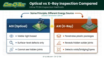
AXI vs. AOI: Both methods rely on the same basic principle: capturing an image and comparing it against a known-good pattern. The difference is the energy source. AOI relies on visible light, so it can only inspect what a camera can see. AXI uses X-rays, which pass through opaque plastic packages and solder masks, letting inspectors see joints that are physically hidden from any camera.
Why PCB Manufacturers Rely on X-Ray Inspection
Component packaging keeps shrinking. Fine-pitch chip-scale packages, package-on-package devices, and imperial 01005 passives create real design and assembly challenges, according to an IPC technical paper on component miniaturization.
As ball grid arrays and QFN packages get smaller and more densely packed, their solder joints end up hidden beneath the component body entirely. There's no way for a camera to verify them.
High-density, high-reliability boards demand more than a good-looking top-side placement. They demand:
- Consistent solder joint integrity across every hidden ball or lead
- Dimensional tolerance that holds up under thermal cycling
- Traceable proof that internal structures meet spec, not just visible ones
Without X-ray verification, defects like solder voids or bridging can slip straight through functional test. A board can power on, pass its electrical checks, and still carry a marginal joint that fails months later in the field.
IPC's own failure-analysis case studies found that solder de-wetting alone accounted for roughly a quarter of the field issues examined. That kind of defect typically hides beneath a component and goes undetected without X-ray review.
Is AXI a Requirement or a Best Practice?
AXI isn't spelled out line-by-line in IPC-A-610, ISO 13485, or IATF 16949. Those standards do require documented process control, monitoring, and nonconforming-product management. AXI is one of the most effective ways to generate that evidence for BGA, QFN, and CSP assemblies. In practice, it's become the default expectation for boards built to Class 3 or medical and automotive requirements.
This is why leading contract manufacturers, including Cir-Q-Tek, build inline AOI and X-ray inspection directly into their SMT lines rather than treating it as an offline extra. Every SMT line runs both inspection types automatically, giving medical and automotive customers a built-in verification step instead of a bolt-on service.
How PCB X-Ray Inspection Works (Step-by-Step Guide)
An X-ray tube emits radiation through the assembled board while a detector on the opposite side captures whatever gets through as a grayscale image. Denser materials — solder, copper leads, metal shields — absorb more radiation and appear dark. Lighter materials like plastics and silicon let more radiation pass through and appear brighter. That contrast is what reveals joint quality.
Operators control the process by adjusting magnification and tilting the board or detector for oblique angles. They also choose between 2D single-shot imaging or 3D methods like tomosynthesis or laminography when boards have double-sided or densely stacked components.
The output is a defect report covering voids, opens, shorts, or misalignment. Each finding is measured against acceptance criteria before the board passes or gets flagged for rework.
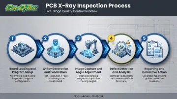
Here's how that plays out across five steps.
Step 1: Board Loading and Program Setup
The fully soldered, reflowed PCB assembly goes onto a movable sample platform inside the X-ray chamber. The operator selects an inspection recipe matched to the board's component mix, whether BGA, QFN, or CSP, along with the defect thresholds that recipe should flag.
Step 2: X-Ray Generation and Penetration
The X-ray tube generates radiation that penetrates the board's layers, components, and solder joints. Absorption varies with material density, producing the contrast that makes hidden joint defects visible on the detector.
Step 3: Image Capture and Angle Adjustment
The detector on the opposite side captures a 2D image of what passed through. When components sit directly over the joints of interest, operators use tilt, rotation, or full 3D CT/laminography scanning to separate overlapping structures and get a clear view of the joint underneath.
Step 4: Defect Detection and Analysis
Image-analysis software compares the captured images against the acceptance criteria loaded during setup, often based on IPC-A-610 void percentage guidance, customer-specific specs, or a calibrated internal recipe. Joints outside the acceptable range get flagged automatically.
Step 5: Reporting and Corrective Action
Flagged boards route to rework, root-cause investigation, or a reflow profile adjustment before anything ships. This closes the loop between what the X-ray found and what the production line changes going forward.
Applications, Key Factors, and Limitations of PCB X-Ray Inspection
Where X-Ray Inspection Is Applied
AXI shows up in three main settings:
- SMT production lines — inline, immediately after reflow soldering, checking boards as they come off the line
- BGA/CSP assembly verification — sample-based QA checks on high-density boards
- Failure-analysis labs — post-failure root-cause investigation when a board fails in the field or during functional test
Some of this is recurring, since every board on a production line gets scanned. Some of it is condition-based, triggered by a customer spec, a suspected defect, or a new component qualification.
Key Factors That Affect Results
Image quality and defect visibility depend on a handful of variables:
- Component density — tightly packed boards create overlapping shadows that make individual joints harder to isolate
- Resolution and magnification — fine-pitch BGA and CSP inspection needs tighter resolution and higher magnification than standard SMT
- 2D vs. 3D systems — 2D is faster and cheaper for screening; 3D confirms suspected issues and separates stacked or double-sided joints
- Inline vs. offline operation — inline systems favor speed and full coverage; offline systems allow more setup time per board at the cost of throughput
Misconceptions and Limitations
A few misconceptions come up often enough to address directly:
- AXI replaces AOI. It doesn't. AOI catches surface-level defects — missing components, wrong polarity, visible bridging — that AXI isn't designed to check.
- Any visible void means a failed board. Not necessarily. IPC standards define acceptable void percentage thresholds by component and class, so a void in the image isn't automatically a reject.
- Raw X-ray images are self-explanatory. They're not. Distinguishing a genuine defect from a normal material shadow takes trained operators or calibrated software.
AXI also isn't always the right call:
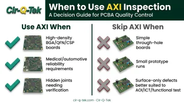
- Simple, low-density through-hole boards with fully visible joints rarely need it — a trained eye or AOI can verify those connections
- Small prototype runs sometimes can't justify the cost and throughput hit of 100% X-ray inspection
- Surface defects and electrical performance are better left to AOI, ICT, or functional test; AXI works best alongside these methods, not instead of them
Conclusion
PCB X-ray inspection is a non-destructive way to see what optical methods cannot see: solder joints and internal structures buried beneath the component body. As packages shrink and industries like medical and automotive demand documented, defect-free reliability, that visibility becomes essential.
The key is applying AXI correctly—as one layer in a broader, ISO-certified quality process, not as a default checkbox on every RFQ. Partners like Cir-Q-Tek build inline AOI and X-ray inspection directly into their SMT lines, giving customers that layered assurance without requiring their own capital investment in inspection equipment.
Frequently Asked Questions
What defects can X-ray inspection detect that AOI cannot?
AXI sees solder voids, BGA/CSP shorts, and open connections hidden beneath components — defects that AOI can't detect because the joint is physically blocked from the camera's view.
Is X-ray inspection safe for PCBs and operators?
Yes. AXI is non-destructive to the board, and enclosed, shielded cabinet systems keep radiation emissions within strict limits set by the FDA, making it safe for operators.
What's the difference between 2D and 3D X-ray inspection?
2D captures a single flat image, similar to a standard bone X-ray. 3D systems build cross-sectional images through CT or laminography, useful for densely stacked or double-sided boards where joints overlap.
How much does PCB X-ray inspection add to manufacturing cost?
It depends on whether the system runs inline or offline and how much volume it processes. For high-density, high-reliability boards, the cost is typically justified, since field failures cost far more to fix than catching a defect before shipment.
At what stage of PCB assembly is X-ray inspection performed?
Most commonly, inline immediately after reflow soldering. Some manufacturers add sample-based checks or run additional X-ray inspection during failure-analysis investigations.
Can X-ray inspection find defects beyond solder joints, like internal via issues?
Yes. AXI can catch pin-hole fill problems in through-hole and via connections, along with certain internal trace or lamination issues, in addition to standard solder joint defects.