Introduction
Look inside a smartphone, an industrial robot, or a car's dashboard, and you'll find the same thing: a green (or sometimes blue or black) board laced with copper pathways. That's the printed circuit board, and it's the nervous system connecting every component in modern electronics.
The market reflects just how central PCBs have become. Fortune Business Insights values the global PCB market at $74.12 billion in 2025, growing at a 6.65% CAGR through 2034.
Yet many engineers, procurement teams, and OEMs still jump into sourcing without understanding PCB basics. That gap leads to costly design revisions and mismatched vendor selections.
This guide breaks down what a PCB actually is, how it's manufactured, the types available, common applications, and how to choose a manufacturing partner that won't slow down your timeline.
Key Takeaways
- A PCB is a laminated board of substrate and copper that supports and electrically connects components
- Boards are classified by layer count (single, double, multilayer) and flexibility (rigid, flex, rigid-flex)
- Manufacturing covers layering, etching, drilling, plating, solder mask, and multi-stage inspection
- Choose a certified partner with quick-turn prototypes to cut risk and speed time-to-market
What Is a Printed Circuit Board (PCB)?
A printed circuit board is a flat, non-conductive board, typically made from fiberglass-reinforced epoxy known as FR-4, with copper pathways etched onto its surface. Those pathways route electrical signals and power between components without relying on loose point-to-point wires.
Every PCB relies on a handful of core elements:
- Traces: etched copper lines that carry electrical current between points
- Pads: small copper areas where components are soldered onto the board
- Vias: plated holes that connect copper layers vertically through the board
- Solder mask: the protective coating (usually green) that prevents unwanted solder bridges
- Silkscreen: printed text and symbols that label components and orientation
From Point-to-Point Wiring to Printed Circuits
Before PCBs existed, electronics were built with point-to-point wiring, hand-soldered connections strung between components one at a time. According to Britannica, printed circuits largely replaced this conventional wiring in radio, television, computer, and guided-missile equipment after World War II. The change cut size and weight while improving reliability and manufacturing uniformity—and it made mass-produced electronics practical.
PCB vs. PCBA: Know the Difference
A PCB is the bare, unpopulated board: substrate and copper only, with nothing mounted yet. A PCBA (Printed Circuit Board Assembly) is that same board after components—resistors, capacitors, chips—have been soldered in place. Sourcing teams often confuse the two terms, which leads to quoting mismatches with vendors.
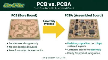
PCBs sit at the foundation of nearly every OEM sector, from medical devices to automotive systems. The sections below break down board types, materials, and manufacturing choices that affect cost, reliability, and lead time.
PCB Composition and Manufacturing Process
Think of a PCB as a layered sandwich: substrate on the inside, copper wrapped around it, then solder mask and silkscreen on top. Each layer plays a distinct structural or functional role.
Layer-by-Layer Composition
The substrate, most commonly FR-4 fiberglass, provides electrical insulation, mechanical strength, and thermal stability. Bonded to it is a copper foil layer, with thickness measured in ounces per square foot rather than inches. A nominal 1-ounce copper layer runs about 0.00135 inches (34 microns) thick.
Over the copper sits the solder mask, the familiar green (or other color) coating that insulates traces and leaves only the pads exposed for soldering. On top of that, the silkscreen prints reference designators, logos, and assembly markings so components can be placed and serviced correctly.
Board complexity comes down to how many copper layers are stacked:
- Single-layer boards carry one copper layer, sufficient for simple circuits
- Double-layer boards add copper on both sides, connected through plated holes
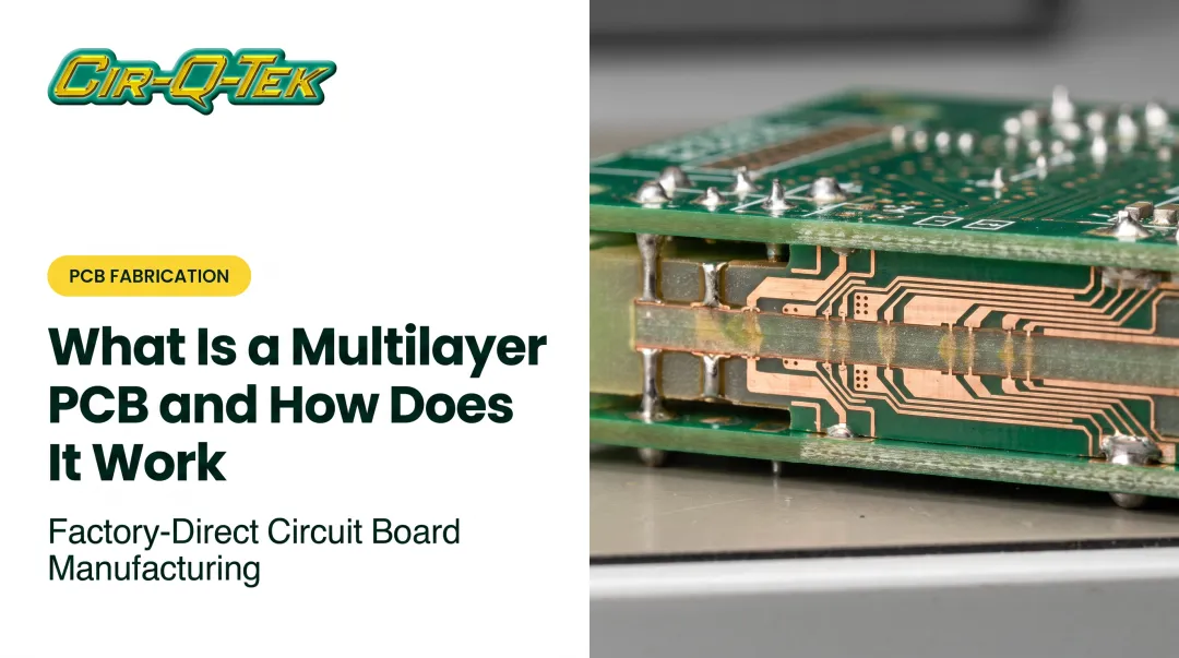
- Multilayer boards stack three or more copper layers for dense routing, high-speed signals, or tight layouts
The PCB Manufacturing Process, Step-by-Step
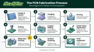
Fabricating a bare board follows a consistent sequence, though multilayer and HDI designs may repeat certain steps:
- Design and layout — Engineers finalize the circuit design and generate Gerber files
- Imaging — Photoresist is applied and exposed to transfer the circuit pattern onto copper
- Etching — Unwanted copper is chemically removed, leaving only the intended traces
- Drilling — Holes are drilled for vias and component mounting
- Copper plating — Drilled holes and outer layers are plated to establish electrical connections
- Solder mask application — A protective coating is applied over exposed copper
- Silkscreen printing — Labels and reference markings are printed onto the board
- Surface finishing — A finish (such as HASL or ENIG) is applied to protect exposed pads
- Final inspection — Electrical and visual testing confirm the board meets specification
Advanced fabrication uses laser direct imaging, automated optical inspection (AOI), and X-ray inspection to catch defects at each stage rather than after the fact. Cir-Q-Tek fabricates multilayer boards up to 40 layers with that class of process control.
Those same inspection tools carry into assembly: its SMT lines run inline AOI and X-ray, which matters most on fine-pitch parts such as 0.2mm BGA packages, where hidden solder joints can't be verified by eye.
Types of Printed Circuit Boards
PCBs are generally sorted two ways: by how many copper layers they contain, and by how rigid or flexible the board itself is. The right choice depends entirely on what the end product needs to do.
By Number of Layers
- Single-sided PCBs — One copper layer, low-cost, and common in simple electronics like calculators and remote controls
- Double-sided PCBs — Copper on both sides connected via through-holes, used in power supplies and HVAC controls
- Multilayer PCBs — Three or more copper layers for dense, high-performance designs in smartphones, servers, and medical equipment
By Flexibility
Layer count isn't the only variable. Whether a board bends, and how, changes what it can be used for:
- Rigid PCBs — Built on a solid, non-bending substrate; think computer motherboards
- Flexible PCBs — Made from bendable materials like polyimide, ideal for wearables and compact devices where space is tight
- Rigid-flex PCBs — Hybrid boards with rigid sections and flexible connectors; common in aerospace systems and medical implants
Rigid-flex construction shows up in demanding environments. NASA's JPL has used rigid-flex boards as primary structural elements in its PUFFER exploration robots, cutting weight and volume in a design that folds like origami.
Medical device makers apply the same logic inside pacemakers and neurostimulators, where every cubic millimeter counts.
Where Are PCBs Used? Common Applications Across Industries
PCBs show up anywhere electronics need to function reliably in a compact footprint. Common applications include:
- Consumer electronics and computing — Smartphones, laptops, and TVs rely on compact multilayer boards to pack more function into less space
- Medical, automotive, and industrial — Patient monitors, ADAS modules, and factory controls need boards built to strict reliability standards, often under ISO 13485 or IATF 16949
- Telecom and emerging tech — Routers, 5G infrastructure, and IoT devices depend on boards engineered for high-speed signal integrity
That last segment is growing fast. Mordor Intelligence forecasts the 5G PCB market rising from $20.25 billion in 2025 to $36.18 billion by 2030 (12.31% CAGR), with IoT and edge devices expanding even quicker inside that mix.
Each application sets different limits on cost, layer count, and certification — so board specs and supplier capabilities have to match the end market, not a generic template.
How to Choose the Right PCB Manufacturing Partner
Price per board is only one factor. Certifications, turnaround speed, and operating model determine whether boards ship on time and meet spec.
Match Certifications to Your Industry
| Certification | What It Covers | Relevant Industries |
|---|---|---|
| ISO 9001 | General quality management systems | All sectors |
| ISO 13485 | Medical device quality requirements | Medical, healthcare |
| IATF 16949 | Automotive quality management | Automotive |
| UL/cUL | Safety compliance approval | US/Canada commercial markets |
Match the fabricator’s certs to your end market so you are not juggling separate suppliers for regulated work. Cir-Q-Tek, for example, holds ISO 9001, ISO 13485, and IATF 16949, plus UL and cUL approval—coverage that supports medical, automotive, telecom, and industrial process control programs under one partner.
Evaluate Turnaround Capability
Once compliance is covered, check whether the shop can keep your launch schedule. Look for fabricators that offer:
- Quick-turn prototypes in about 5 days total (Cir-Q-Tek builds in 3 days and ships within 2)
- Production runs on a clear 10-day to 4-week window by layer count, board type, and material lead time
- No rigid minimums, so small batches and volume ramps use the same partner
Consider a Domestic-Offshore Hybrid Model
Speed and certs still fall short if cost and communication pull in opposite directions. A hybrid partner pairs offshore production pricing with a U.S. service desk and bilingual coordination.
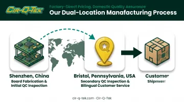
Cir-Q-Tek runs that model from Bristol, Pennsylvania (secondary QC and customer service) and Shenzhen, China (manufacturing access). Boards are inspected at the factory, then again domestically before shipment—catching issues a single-location supplier can miss.
Frequently Asked Questions
What does PCB stand for in a circuit board?
PCB stands for "printed circuit board," sometimes called a "printed wiring board" (PWB). It refers to the etched copper-and-substrate board used to connect electronic components.
How much does a PCB circuit board cost?
Cost varies widely based on size, layer count, material, and order volume. Simple single-layer boards can cost just a few dollars each; complex multilayer boards cost significantly more. Request a quote for accurate pricing on your design.
What is the difference between a PCB and a PCBA?
A PCB is the bare, unpopulated board. A PCBA is that same board after components have been soldered onto it during the assembly process.
How many layers can a PCB have?
Most common applications use boards ranging from 1 to 8 layers. Advanced designs for aerospace or data centers can exceed 30 to 40 layers, depending on the fabricator's capability.
What materials are PCBs made from?
Most PCBs use FR-4 fiberglass substrate paired with copper layers. Specialty boards may use aluminum, polyimide, or PTFE for specific thermal management or high-frequency performance needs.
How long does PCB manufacturing typically take?
Prototype boards can often be completed in a few days. Full production runs typically take 10 days to 4 weeks, depending on complexity, quantity, and layer count.