ICT gets referenced constantly in supplier conversations, but it's rarely explained at the level that actually matters: how the fixture works, what the software checks, and why some boards simply can't be tested this way. This article covers how ICT works, why manufacturers use it, what determines whether it performs well on your board, and when it's the wrong tool for the job.
Key Takeaways
- ICT uses a bed-of-nails fixture to verify shorts, opens, resistance, capacitance, and part placement on a populated board
- Cost-effective for medium-to-high-volume, stable designs — not low-volume prototypes
- Fast, repeatable, high-coverage testing comes with a real upfront cost in custom fixtures and programming
- Design-for-testability (probe pads, tooling holes, spacing) directly caps how much coverage ICT can achieve
- Best results come from pairing ICT with AOI, X-ray, and functional testing, not as a standalone check
What Is In-Circuit Testing (ICT) for PCB Assembly?
ICT is an automated, fixture-based test that makes direct electrical contact with individual test points on a populated PCB to verify each component's placement, value, and connectivity. A tester applies controlled signals through spring-loaded probes and reads back measurements against a stored specification for that board.
The goal is straightforward: catch component-level defects (a wrong resistor value, a missing capacitor, a solder short between adjacent pads) before the board advances to functional test or final assembly. Catching these issues early is far cheaper than discovering them after a unit ships.
ICT isn't the only PCB test method, and this table shows where it sits relative to close relatives:
| Method | Contact type | Best fit |
|---|---|---|
| ICT | Fixed bed-of-nails probes, all points simultaneously | High-volume, stable designs |
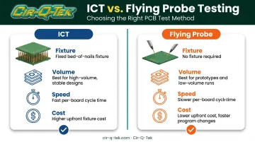
| Flying probe | Movable probes, no fixture required | Prototypes, low-volume, frequent revisions |
| AOI / X-ray | Optical or imaging-based, no electrical contact | Solder joint and placement verification, including hidden BGA joints |
Flying probe trades speed for flexibility: no fixture means faster program changes but slower per-board cycle times. AOI and X-ray inspect visually or through imaging rather than measuring electrical values directly, which is why they catch different defect types than ICT does.
Why ICT Is Used in PCB Assembly
Manufacturers adopt ICT primarily because it delivers fast, highly repeatable electrical verification down to the individual component. On a stable, high-volume production line, that consistency across thousands of identical boards is worth the setup cost.
What PCB assembly demands, and what ICT delivers:
- Precise fault localization: a failed net points directly to the defective component
- High test coverage across resistors, capacitors, ICs, and connectors in a single pass
- Consistent results board after board, without operator-dependent variability
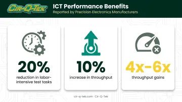
Keysight reports that ICT cut labor-intensive test tasks by 20% and raised throughput by 10% on an automotive ADAS assembly line. Other manufacturers have seen throughput gains of 4x to 6x after adopting ICT systems.
Without adequate electrical testing, defects surface later in the product life cycle, when they cost far more to fix. Common consequences include:
- Undetected shorts or opens that pass initial power-on but fail intermittently
- Misplaced or wrong-value components that only show up under specific operating conditions
- Solder defects (opens, cold joints) that manifest as field failures months after shipment
ICT is largely an operational best practice rather than a regulatory mandate. No IPC or IATF document names ICT as universally required. That said, it's especially valued in regulated sectors like medical and automotive PCBA, where fault localization and repeatability support the broader quality documentation those industries demand.
Comprehensive contract manufacturers layer ICT with other inline inspection methods rather than relying on it alone. Cir-Q-Tek's SMT lines, for example, run inline AOI and X-ray on every line. Those methods complement electrical testing like ICT by catching solder joint and placement issues that probing alone can miss.
How ICT Works (Conceptual Flow)
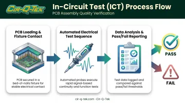
ICT follows a simple loop: load a populated board into a custom fixture, apply controlled signals through spring-loaded probes, capture measurements, and compare results against a programmed pass/fail spec.
Three things must be in place first:
- A fully assembled PCB
- A fixture engineered to that board's exact layout
- Test software programmed with expected values for every net
Step 1: PCB Loading and Fixture Contact
The assembled board is aligned and pressed onto the bed-of-nails fixture. In fixtureless setups, flying probes make contact instead. Either way, the goal is secure electrical contact with every designated test net before measurement begins.
Step 2: Automated Electrical Test Sequence
Once contact is established, the system runs a programmed test sequence. Typical checks include:
- Shorts and opens
- Passive component values (resistance, capacitance, inductance)
- Powered analog and digital checks
- Boundary scan for devices with limited physical probe access (in some setups)
Software controls the order. Checking for shorts before applying power protects both the board and the fixture.
Step 3: Data Analysis and Pass/Fail Reporting
Captured measurements are compared against specification limits stored in the test program. The system generates a report flagging any failed nets or components. Failed boards route to rework stations rather than continuing down the line. Boards that pass move on to functional test or final assembly with a documented electrical pass status attached.
Where ICT Is Applied & Key Factors That Affect It
ICT typically runs right after SMT reflow and before functional or system-level testing, as an inline checkpoint on the production floor rather than a one-off audit. Shops apply it to every board (or a statistically sampled subset), not only when a specific fault condition appears.
Several factors determine how well ICT actually performs on a given board:
- PCB layout and design-for-testability: probe-able pads, tooling holes, and test point spacing set the coverage ceiling
- Component density and miniaturization: fine-pitch parts, BGAs, QFNs, and CSPs limit probe access and cut coverage
- Fixture quality and probe maintenance: worn or misaligned probes create measurement drift over long runs
- Production volume and lifecycle length: these decide whether the fixture investment pays off
- Industry-specific requirements: medical and automotive PCBAs often need higher coverage and documented traceability
Board layout matters more than most people expect here. Anzer's design-for-testability guidance specifies a minimum 40 mil (1.0 mm) test pad diameter with 50 mil preferred, and 50 mil minimum center-to-center spacing between test points, with 75–100 mil recommended for standard-density boards. Skip these clearances at layout time, and no amount of programming skill fixes it later.
Regulated builds also need a partner who can pair ICT with complementary inspection and the right paperwork trail. Cir-Q-Tek runs advanced SMT with ISO 13485 and IATF 16949 certified processes, which helps align coverage and documentation for medical and automotive PCBAs.
If you're setting test strategy for a regulated board, request a quote early enough to get design feedback before layout is locked.
Common Issues, Misconceptions & When ICT Isn't the Right Fit
"ICT confirms the board works." Not quite. ICT verifies that individual components are correctly placed and valued, not that the components interact correctly as a system. That's what functional testing is for. A board can pass ICT with flying colors and still fail to boot.
"ICT can test any design." Coverage depends heavily on whether the board was designed with test-point access in mind. Skip the design-for-testability step, and even a well-programmed ICT system will have blind spots.
High coverage ≠ zero defects. A 95% coverage figure still leaves 5% of nets untested, and parallel-component configurations can mask a failure even within tested nets. Coverage numbers are useful, but they're not a guarantee.
Those limits on what ICT proves also show up in when it makes sense to use it at all.
When ICT is the wrong tool:
- Low-volume runs, typically under a few thousand units, where fixture cost doesn't pay back
- Rapidly changing prototype designs still going through revisions
- Densely packed boards with fine-pitch or leadless parts lacking test-point access
In these cases, flying probe testing is usually the better alternative: no fixture required, and program changes are faster when the design shifts.
Frequently Asked Questions
What is ICT test in PCB?
ICT, or in-circuit testing, is an automated electrical test that uses a bed-of-nails fixture to check individual components on a populated PCB for correct placement, value, shorts, and opens.
Is ICT testing expensive?
ICT requires significant upfront investment in custom fixtures and programming. It becomes cost-effective per unit at higher volumes but is typically not economical for small or one-off orders.
What are the 7 types of PCB testing methods?
The seven common methods are ICT, flying probe testing, AOI, AXI (X-ray inspection), boundary scan/JTAG, functional testing, and burn-in/environmental stress testing. Most production lines combine several of these rather than relying on one.
How does ICT differ from flying probe testing?
ICT uses a fixed custom fixture for fast, high-volume testing, while flying probe uses movable probes with no fixture requirement. Flying probe is generally better suited for prototypes and low-volume runs where designs still change.
How long does an ICT test take per board?
ICT is typically very fast, often about a minute per board once the fixture and program are set up. That is considerably quicker than flying probe cycle times on comparable boards.
Is ICT suitable for low-volume or prototype PCB assembly?
Generally, no. Fixture setup costs make ICT hard to justify for small or prototype runs. Flying probe testing or AOI is usually the better fit until volumes climb enough to offset the fixture investment.