Introduction
Walk into almost any modern electronics factory and you'll see pick-and-place machines setting tiny components onto bare boards at high speed. Surface mount technology (SMT) now accounts for the vast majority of PCB assembly work — well over 90% of components placed in modern electronics — and is the default method for everything from smartphones to medical monitors.
Engineers and procurement teams face a common problem, though. Sourcing decisions, design choices, and manufacturing partner selection all hinge on understanding SMT fundamentals — and a lot of that knowledge is scattered across outdated forum posts or vendor marketing pages.
This article breaks down what SMT actually is, how it stacks up against through-hole assembly, what the design and manufacturing process looks like in practice, and what to check before handing your board to a contract manufacturer.
Key Takeaways
- SMT mounts parts on surface pads, enabling smaller, denser boards than through-hole
- Shorter SMT leads cut parasitic inductance for RF and high-speed signal integrity
- Most production boards mix SMT and through-hole on the same assembly
- Vet partners on ISO certifications, inline inspection, and prototyping speed
What Is Surface Mount Technology (SMT) in PCBs?
Surface mount technology refers to mounting components directly onto pads on the board's surface, rather than inserting leads through drilled holes. The components, often called SMDs or surface mount devices, are soldered in place using a reflow process instead of wave soldering or hand-soldering through-hole leads.
SMT isn't new. It emerged in the 1960s, and by the 1980s it had become the preferred assembly method across many industries as manufacturers pushed for smaller, lighter products. By the end of the century, it was widely used throughout electronics manufacturing.
Common SMD Package Types
Package size drives how dense a board can get. Here's a quick reference for common passive and IC packages:
| Package | Typical Dimensions | Notes |
|---|---|---|
| 0402 | 1.00 x 0.50 mm | Common in space-constrained consumer devices |
| 0603 | 1.60 x 0.80 mm | Balances size with manual rework feasibility |
| 0805 | 2.00 x 1.25 mm | Easier hand-soldering, still compact |
| QFN | Varies by pin count | Leadless, thermally enhanced package |
| BGA | Varies by ball pitch | Solder balls connect substrate to board |
| CSP | ~120% of die area | Nearly die-sized footprint |
Smaller packages like 0402 and below let designers fit far more functionality into the same footprint. That is a big reason wearables and IoT devices keep shrinking while gaining features.
Density and Automation
SMT allows components on both sides of a board, something through-hole assembly can't easily replicate. Combined with automated pick-and-place equipment and smaller component sizes, this yields higher component density per square inch than through-hole designs, according to a manufacturing comparison from MacroFab.
That density advantage is why SMT underpins compact electronics: smartphones, medical wearables, industrial sensors, and IoT modules all depend on it.
Surface Mount vs. Through-Hole PCB: Key Differences
The mechanical difference is straightforward. Through-hole (THT) leads pass through drilled holes and are soldered on the opposite side of the board. SMT components sit flush on surface pads and are attached through reflow soldering, with no drilling required.
That single difference cascades into several practical distinctions:
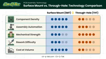
| Factor | SMT | Through-Hole |
|---|---|---|
| Component density | High — both sides usable | Lower — holes limit placement |
| Assembly automation | Nearly fully automated | Slower, more manual intervention |
| Mechanical strength | Solder-joint only | Stronger bond from inserted leads |
| Rework difficulty | Harder on fine-pitch parts | Generally easier to rework |
| Cost at volume | Lower per board at scale | Higher labor cost at scale |
As EE Times notes, SMT lines can run almost fully automated with a lower cost per board at volume, while through-hole leads create a stronger mechanical bond. That trade-off between speed and density versus mechanical robustness drives most design decisions.
Electrical Performance
Shorter leads matter more than people expect. Reduced lead length in SMT components lowers parasitic inductance, which improves signal integrity in high-frequency designs. Texas Instruments notes that leaded capacitors generally become self-resonant around 80 MHz, a limitation that surface mount parts largely avoid thanks to their shorter, more direct connections.
When to choose which:
- SMT: compact products, high-volume automated production, RF or high-speed designs
- THT: connectors, heavy or high-stress components, boards needing easier prototyping and manual rework
Mixed-Technology Assembly
Most production boards don't pick one method exclusively. They combine SMT for logic and signal circuits with through-hole for connectors or power components that need extra mechanical strength, such as board-mounted terminal blocks or large electrolytic capacitors.
When a board uses both technologies, the assembly sequence matters. Populating components on both sides through reflow requires careful planning so heavier through-hole parts don't shift or fall during a second reflow pass. This is one reason experienced contract manufacturers plan the reflow sequence before committing to a stencil design.
The Surface Mount PCB Design Process
Getting SMT right starts long before parts hit the board. The design phase determines whether your assembly runs smoothly or generates costly defects.
Schematic Capture and Component Selection
Design begins with schematic creation, where engineers select SMD footprints and packages matched to the target board size and expected assembly volume. Choosing 0402 passives for a high-volume consumer product makes sense; the same choice on a low-volume prototype board with manual rework needs might create unnecessary headaches.
Layout, Placement, and Routing Best Practices
Once the schematic is locked, layout decisions shape manufacturability:
- Functional grouping — separate power, analog, and digital sections to reduce noise coupling
- Spacing clearances — leave enough room between fine-pitch components for stencil and placement tolerances
- Thermal management — use copper pours and thermal vias to pull heat away from dense component clusters
- Fiducial marks — place these reference points so pick-and-place equipment can locate the board precisely
Routing brings its own rules. Trace width and spacing must match current and voltage requirements. BGA fan-out often relies on via-in-pad techniques to route dense ball grids without running out of board real estate. High-speed signals need controlled impedance routing to avoid reflections and signal loss.
Manufacturing-Ready Design Considerations
Before a design goes to fabrication, a few decisions most affect solderability, flatness, and yield.
Surface finish selection affects solderability and reliability, especially for fine-pitch parts:
- ENIG — flat, reliable surface well-suited to fine-pitch and BGA work
- Immersion Silver — coplanar finish that supports tight-pitch assembly
- OSP — cost-effective but needs careful paste overprint for full wetting
- HASL — economical but less flat, which can complicate fine-pitch soldering
Cir-Q-Tek offers all four of these finishes, plus immersion tin and lead-free HASL, across its PCB fabrication lines. That range lets engineers match finish to the application and pitch requirements.
Symmetrical stack-ups matter for reflow stability. An unbalanced layer structure can warp or twist during reflow's thermal cycling, throwing off component placement on boards that looked perfectly flat on the CAD screen.
Finally, run DRC and ERC checks before generating Gerber files. Catching spacing violations and unconnected nets at this stage costs minutes; catching them after boards are fabricated costs weeks.
Surface Mount PCB Assembly Process
The physical assembly process follows a consistent sequence, regardless of board complexity.
- Solder paste stencil printing — paste is deposited onto pads through a precisely cut stencil
- Automated pick-and-place — machines position components onto the wet paste at high speed
- Reflow soldering — boards pass through a controlled thermal profile: preheat, soak, reflow, and cooling
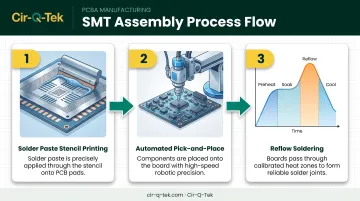
Each stage has to work correctly for the next to succeed. Get the stencil aperture wrong, and placement accuracy won't save a joint that never had enough paste.
Quality Inspection Methods
Three inspection methods catch problems at different stages:
- SPI (Solder Paste Inspection) — verifies paste volume and placement before components go on
- AOI (Automated Optical Inspection) — checks placement accuracy and visible solder joint quality
- X-ray inspection — reveals hidden joints under BGA and QFN packages that AOI can't see
Cir-Q-Tek's SMT lines run inline AOI and X-ray inspection at each stage of assembly, rather than treating inspection as a separate offline step. Catching a placement error before reflow is far cheaper than discovering it after a finished board fails functional test.
Common Defects and Their Causes
- Tombstoning — one component termination wets before the other, lifting the part upright
- Bridging — excess paste overflows and connects adjacent pads
- Insufficient solder — often traced to stencil misalignment or paste viscosity issues
- Voiding — trapped volatiles or reflow-profile errors leave gaps inside the joint
Proper stencil design and a well-calibrated reflow profile prevent most of these issues before they ever reach inspection.
Benefits and Design Trade-Offs of SMT
SMT's advantages explain why it dominates modern production:
- Higher component density, enabling smaller and lighter boards
- Faster automated assembly with less manual labor
- Better high-frequency electrical performance from reduced lead parasitics
- Support for double-sided population, maximizing board real estate
Those gains come with real design and process costs:
- Rework and prototyping need finer tools and skill — a fine-pitch QFN is not a soldering-iron fix
- Fine-pitch joints are more sensitive to thermal cycling, especially in automotive and industrial temperature swings
- Placement accuracy and inspection (AOI, X-ray) matter more as pitch shrinks
Weigh density, assembly volume, operating environment, and rework access against each other before you lock the package set.
Choosing the Right Manufacturing Partner for Surface Mount PCBs
Not every contract manufacturer handles fine-pitch SMT equally well. A few criteria separate the qualified partners from the rest.
Evaluate potential partners on:
- ISO certifications — ISO 9001 for general quality management, ISO 13485 if you're building medical devices, IATF 16949 for automotive programs
- Inline inspection capability — AOI and X-ray built into the line, not bolted on as an afterthought
- Quick-turn prototyping speed — how fast can they turn a design into a physical board you can test?
Cir-Q-Tek is built to clear those bars as a one-stop PCB and PCBA partner: domestic-level service at offshore pricing. Quick-turn SMT prototypes take 3 days to build and 2 days to ship, which matters when a design review is holding up your entire product timeline. Full production runs, by comparison, typically take 10 days to 4 weeks depending on complexity and volume.
On the technical side, Cir-Q-Tek's lines process ultra-fine components including 01005 passives, BGAs with 0.2mm ball spacing, QFN, and CSP packages, on boards up to 40 layers. That combination covers most of what a modern high-density design throws at a manufacturer.
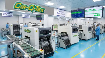
Those same ISO 9001, ISO 13485, and IATF 16949 certifications mean medical and automotive boards don't need a separate qualified line.
The dual-office structure pairs a U.S. headquarters in Bristol, Pennsylvania with a Shenzhen, China office staffed by bilingual personnel. Specs and design intent move without the translation gaps that derail many offshore relationships.
Boards also get a second quality inspection at the Pennsylvania facility before they ship to customers.
If you're weighing a new SMT project, request a quote with your Gerber package and BOM for a straight answer on timeline and cost.
Frequently Asked Questions
What is surface mount in PCB?
Surface mount is the process of soldering components directly onto pads on a board's surface, without drilling holes for leads. Through-hole mounting, by contrast, requires leads to pass through the board and be soldered on the opposite side.
What are the key differences between surface-mount and through-hole PCBs?
SMT offers higher component density, faster automated assembly, and better high-frequency performance. Through-hole provides stronger mechanical bonds and easier manual rework, making it better suited to connectors and heavy components.
Can SMT and through-hole components be used on the same PCB?
Yes, mixed-technology assembly is common. Most production boards use SMT for logic and signal circuits while reserving through-hole for connectors or power components that need extra mechanical strength.
What are common SMD package sizes?
Typical passive component sizes include 0402, 0603, and 0805, measured in hundredths of an inch. High-density designs increasingly use even smaller packages like 0201 and 01005 to maximize board space.
What is a PCB stencil used for in SMT assembly?
A stencil applies precise solder paste deposits onto board pads before components get placed. Accurate paste volume from the stencil is one of the biggest factors in avoiding bridging, insufficient solder, and other reflow defects.
What inspection methods ensure SMT assembly quality?
SPI checks solder paste volume before placement, AOI verifies visible placement accuracy after components are mounted, and X-ray inspection reveals hidden joints under packages like BGAs and QFNs that other methods can't see.