
The stakes are highest earlier than most teams realize. A widely cited figure in manufacturing systems literature puts the number at 80% of a product's total cost committed during the design stage (ASME, 2016). That's not a PCB-specific statistic, but it tracks with what engineers see on the shop floor every day: decisions made at layout ripple through fabrication, assembly, and total cost of ownership.
This guide breaks down the design and assembly mistakes that cause the most rework, and how to catch them before they reach production.
Key Takeaways
- Skipped DFM/DFA reviews, sloppy documentation, and weak thermal planning cause most PCB failures
- Catching errors before fabrication costs far less than fixing boards after they're built
- Accurate BOMs, CPL files, and early design reviews prevent most costly respins
- Choosing an ISO-certified manufacturer with in-house AOI and X-ray inspection cuts risk at every stage
What Is PCB Design and Assembly?
PCB design is the layout and schematic phase: component placement, routing, and stack-up definition. This is where the circuit takes physical shape on the board before anything gets built.
PCB assembly (PCBA) happens after fabrication. It's the process of populating the finished board with components through surface-mount technology (SMT), through-hole technology (THT), and soldering.
Design errors rarely surface during design. They show up during fabrication or assembly, when a footprint doesn't match a datasheet or a trace violates clearance rules the fabricator can't work around. By then, fixing the issue means new tooling, new stencils, or a full respin.
Two disciplines prevent this:
- DFM (Design for Manufacture): Design rules that keep the board within current fabrication process limits
- DFA (Design for Assembly): Design rules that keep the board within current assembly process limits (Altium, 2025)
Skip either one, and most of the mistakes that follow become far more likely.
Common PCB Design Mistakes to Avoid
Most PCB failures that surface in fab or assembly start as preventable layout choices. Catching them early avoids respins, scrap, and slipped launch dates.
Skipping DFM/DFA Reviews Before Finalizing the Layout
Designers who lock in a layout without a DFM/DFA check often discover fabrication or assembly conflicts only after boards are already built. At that point, the fix isn't a quick edit. It's a respin.
The cheaper path: request a DFM/DFA review before committing files to production. A manufacturing partner can flag issues like insufficient clearance, unsupported drill sizes, or placement conflicts while changes still cost nothing but time.
Inadequate Trace Spacing and Clearance Violations
Trace-to-trace spacing controls crosstalk and electromagnetic interference (EMI). One common guideline, the 3W rule, suggests spacing trace centers at least three times the trace width apart to reduce inductive coupling.
Treat 3W as a starting heuristic, not a hard spec. EDA sources disagree on the exact reference point, and some geometries perform fine at 1.5W or 2W once simulated. Run a field solver or crosstalk simulation against your actual stack-up instead of assuming a rule of thumb covers every design.
Incorrect Component Footprints and Pad Design
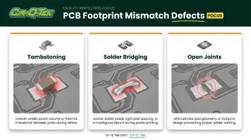
Footprints that don't match the manufacturer's datasheet, whether the pad size, spacing, or orientation is off, create predictable assembly failures:
- Tombstoning: one end of a passive lifts off the pad during reflow
- Solder bridging: excess paste connects adjacent pads
- Open joints: mismatched courtyard or pad geometry prevents proper wetting
Fine-pitch packages amplify the risk. QFN and SON components, for example, need clearance and pad width dialed in tightly to the package specification, not a generic library default.
Poor Thermal Management and Via Planning
Power-dense designs generate heat that has to go somewhere. Skimping on thermal vias, copper pour, or heat-sink pathways invites overheating and shortened component life.
The PCB itself can act as a heat-dissipation structure when designed correctly. Copper planes, thermal vias sized and spaced for the package, and generous copper on multiple layers pull heat away from hot components and protect long-term reliability.
Neglecting Manufacturability in Component Placement
Placement decisions that look fine on screen can create real headaches on the assembly line:
- Crowding parts near board edges limits clearance for pick-and-place nozzles and tooling
- Mixing orientations without a need slows machine placement and adds setup complexity
- Overlooking assembler equipment limits forces manual workarounds that raise cost and defect risk
This is DFM/DFA in practice: design decisions made with the assembly floor in mind, not just the schematic.
Common PCB Assembly Mistakes to Avoid
Even a solid PCB layout fails in production when assembly files, parts, or process steps are wrong. These are the assembly mistakes that most often stall builds, create defects, or push failures into the field.
Incomplete or Inaccurate BOM and CPL Files
A Bill of Materials with missing manufacturer part numbers (MPNs), wrong reference designators, or outdated quantities can stall procurement before assembly even starts.
The Component Placement List (CPL) carries its own risk: outdated pick-and-place coordinates mean components land in the wrong spot, rotated the wrong way, or on the wrong side of the board.
Both files need to match the released PCB revision exactly. A BOM or CPL that references an earlier design iteration builds boards to specifications nobody intended to ship.
Sourcing Unreliable or Counterfeit Components
Buying from unverified suppliers, or missing that a part has gone end-of-life (EOL), opens the door to field failures that surface long after the board ships.
This isn't a rare problem: ERAI logged 1,055 suspect counterfeit and nonconforming parts in 2024, a 25% increase over the prior year and the highest total since 2015. Obsolete parts made up the largest share of those reports (ERAI, 2024 Annual Report).
Sourcing from traceable, reputable vendors, and applying counterfeit-risk controls for any open-market purchase, cuts most of that risk.
Improper Solder Paste Application and Reflow Settings
Two things drive most solder defects:
- Stencil aperture design — wrong-sized apertures for the pad geometry cause insufficient or excess paste deposition
- Reflow temperature profile — lead-based and lead-free alloys need different peak temperatures and dwell times; the wrong profile causes bridging, tombstoning, or cold joints
Match aperture design and reflow profile to the specific paste and package in use. A generic, one-size-fits-all setting is how clean boards turn into rework.
Skipping Adequate Inspection Stages
Visual inspection alone misses what it can't see. Hidden BGA and QFN solder joints, in particular, need methods that go beyond the naked eye (Nordson, 2024):
- Automated Optical Inspection (AOI) catches visible defects: misalignment, missing components, solder bridges on accessible pads
- X-ray inspection catches what's hidden underneath: BGA voids, insufficient solder, head-in-pillow defects
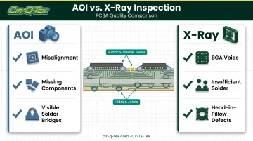
Facilities running inline AOI and X-ray on every SMT line, like Cir-Q-Tek's assembly lines, catch these defects during production rather than after a board fails in the field.
Mixing Assembly Technologies Without a Clear Plan
Boards that combine through-hole and surface-mount components need a deliberate sequence. Reflow, wave soldering, and manual soldering each interact differently with sensitive parts, and running them in the wrong order can damage components or weaken joints that looked fine on inspection.
There's no single universal sequence. The right method depends on component placement and thermal sensitivity:
- Selective wave soldering for mixed-technology boards with clustered through-hole parts
- Pin-in-paste reflow when through-hole parts can share the SMT reflow cycle
- Hand soldering for low-volume parts, connectors, or thermally sensitive components
Documentation and File Preparation Mistakes That Delay Production
Incomplete or inconsistent Gerber or ODB++ files, missing drill data, or absent fiducial markers are among the most common reasons a manufacturer puts a job on hold to request clarification. Every day spent clarifying files is a day added to the schedule.
Revision drift is just as costly. When BOM, CPL, and layout files aren't synchronized across design changes, boards get built to specs that are already outdated. That mismatch shows up often on projects with multiple engineering change orders.
Before submitting a job, run through this checklist:
- Confirm the board outline is closed, with no gaps or overlaps
- Match the layer stack-up to the fabrication drawing exactly
- Include the netlist so Gerber data can be cross-checked
- Document assembly notes: component orientation, non-washable parts, and special soldering instructions
- Verify BOM, CPL, and layout all reference the same design revision
Fix these gaps before you submit, and you keep the build on the original schedule.
Best Practices to Avoid PCB Design and Assembly Mistakes
Most of the mistakes above share a common fix: bring your manufacturing partner in early, not after the design is "final."
- Request a formal DFM/DFA review before committing files. A review at the layout stage catches conflicts while they're still cheap to fix.
- Design with standard components and modular blocks. Standard parts simplify sourcing, speed up testing, and reduce the number of unique assembly steps.
- Work with certified manufacturers for regulated industries. ISO 9001, ISO 13485, and IATF 16949 partners build compliance in from the first design review—not after the fact.
- Choose a one-stop partner over fragmented vendors. When fabrication and assembly happen under one roof, design intent doesn't get lost at the handoff between separate companies.
Cir-Q-Tek's model reflects that last point directly. Fabrication and turnkey assembly run as one integrated process:
- PCB fabrication up to 40 layers with laser direct imaging
- Turnkey PCBA covering SMT, through-hole, and box build
- Quick-turn prototypes built in 3 days and shipped in 2
- Inline AOI and X-ray on every SMT line, plus a secondary check at the Pennsylvania facility before shipment

Design flaws and assembly defects get multiple chances to surface before a board reaches your dock. If you're preparing a new board for production, request a quote with your Gerber package and BOM to start that review.
Frequently Asked Questions
What is PCB design and assembly?
PCB design is the layout and schematic phase, covering component placement, routing, and stack-up. PCB assembly (PCBA) is the physical process of mounting and soldering components onto the fabricated board.
What is the 3W rule in PCB layout?
The 3W rule recommends spacing trace centers at least three times the trace width apart to reduce crosstalk. It's a design rule of thumb, not a fixed IPC tolerance, so simulation against your actual stack-up gives more reliable results.
What are the four stages of PCB design?
The four stages are schematic capture, layout and component placement, routing and stack-up definition, and generating fabrication output files (Gerber or ODB++, drill data, and pick-and-place files).
How can I avoid common PCB assembly mistakes?
Keep your BOM and CPL accurate and synced to the current design revision. Source components from verified suppliers, and request a DFA review with multi-stage inspection (AOI and X-ray) before production.
What is the difference between DFM and DFA?
DFM focuses on optimizing the board so it can be fabricated cost-effectively within current process limits. DFA focuses on optimizing component selection and placement so the board assembles efficiently on the line.
How much more does it cost to fix a PCB mistake after production versus during design?
There's no single universal multiplier, but post-production fixes usually require new tooling, rework, or a full respin. The same issue caught in a DFM/DFA review typically costs only design time.