The numbers back this up. The multilayer PCB market was valued at $29.62 billion in 2024 and is projected to reach $42.61 billion by 2035, according to Market Research Future. That growth reflects a simple reality: single and double-sided boards can no longer keep up with what today's electronics demand.
Yet many engineers and buyers still aren't clear on how these boards are actually built and connected. That confusion leads to design mistakes, sourcing delays, and cost surprises. This guide breaks down exactly what a multilayer PCB is and how it works, stage by stage.
Key Takeaways
- A multilayer PCB stacks three or more copper layers, bonded with insulating prepreg under heat and pressure.
- Vias — through-hole, blind, and buried — carry electrical connections between layers.
- Layer counts are usually even (4, 6, 8...) to avoid warping during lamination.
- Applications span smartphones, medical imaging, automotive control units, and industrial systems.
- Cost and lead time scale directly with layer count, via complexity, and copper weight.
What Is a Multilayer PCB?
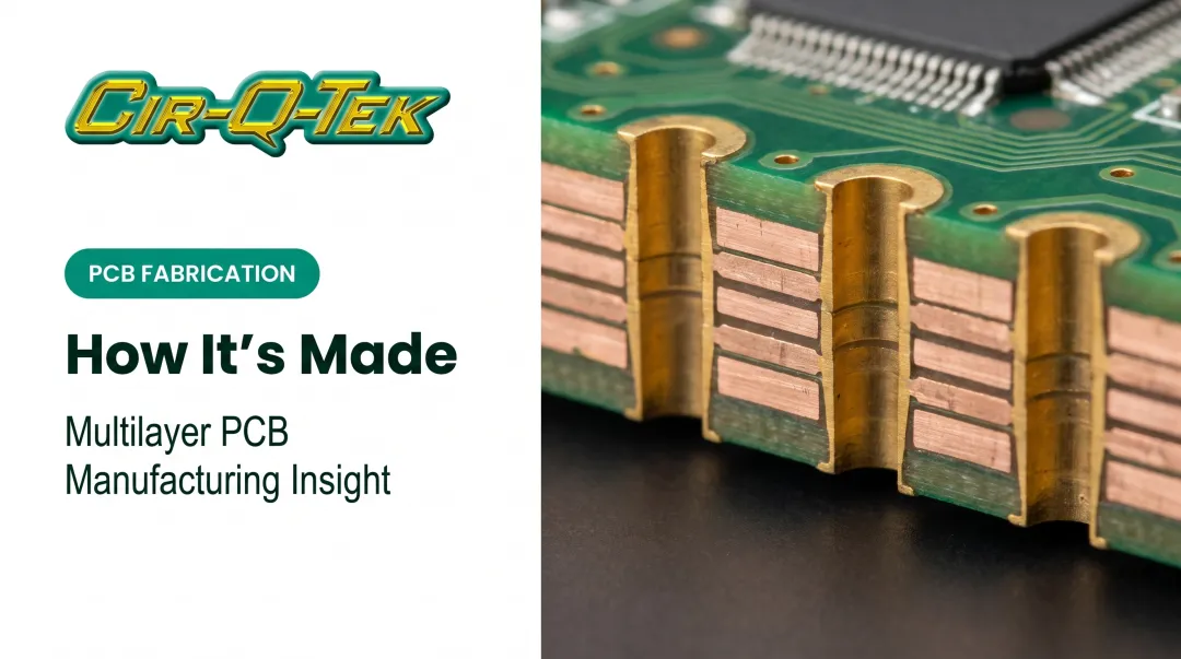
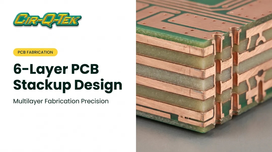
A multilayer PCB is a printed circuit board built from three or more conductive copper layers, separated by insulating dielectric material and laminated together into a single rigid structure. Each inner layer carries its own circuit pattern, connected to the others through drilled and plated vias.
As electronics shrank while packing in more functionality, single and double-sided boards hit a wall. There simply wasn't enough room to route every signal, power, and ground connection on just one or two conductive surfaces. Multilayer construction solved that by moving routing inward, stacking extra copper planes rather than expanding the board's footprint.
Don't confuse a multilayer PCB with a double-sided board. A double-sided board has exactly two conductive layers, with components and traces on the top and bottom only, and no internal stacked circuitry. A multilayer board adds internal copper planes sandwiched between outer layers, which increases wiring density and improves signal integrity and noise control.
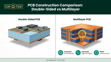
Despite newer packaging options, multilayer PCBs remain the standard. Miniaturization and higher component density keep driving demand, and stacked-layer construction is still the most reliable way to deliver both.
Types and Layer Count Variations
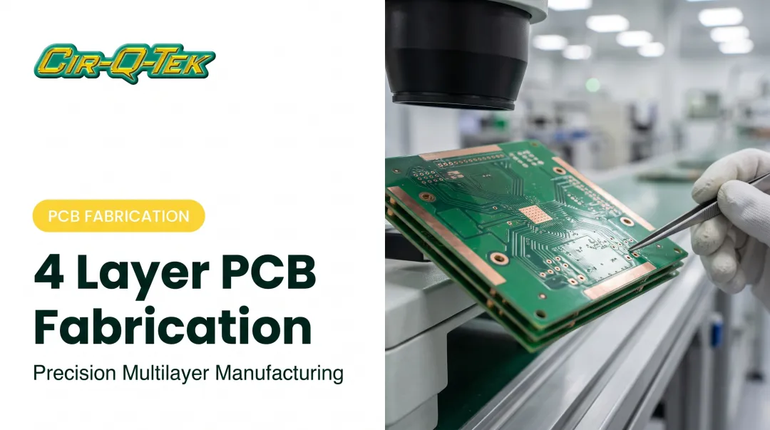
Layer counts almost always land on even numbers, such as 4, 6, 8, or 10. That choice is practical, not arbitrary. Odd-layer stacks are manufacturable but harder to control, because unbalanced lamination raises the risk of warping. A symmetric 4-layer board is simply easier to keep flat than a 3-layer one.
So do three-layer PCBs exist? Yes, but they're rare. Most appear on small, simple boards where the warping risk stays manageable.
Beyond layer count, multilayer PCBs also come in different physical formats:
- Rigid: the standard stiff-board construction most people picture
- Flexible (multilayer flex): bendable substrates for tight or curved enclosures
- Rigid-flex: combines rigid sections with flexible connectors in one assembly
Fabrication complexity climbs with each of these, especially when higher layer counts and flex requirements stack together.
How Does a Multilayer PCB Work?
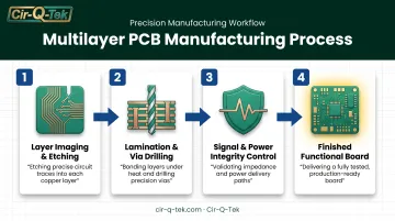
A multilayer PCB comes together through a defined sequence: build individual layers, laminate and bond them, connect them electrically with vias, then control signal and power integrity across the finished stack. Here's how each stage plays out.
Initiation: Building the Individual Layers
Before any stacking happens, each copper-clad core gets its own circuit pattern. This starts with photo-imaging, where a light-sensitive film is exposed to a circuit design, followed by developing, etching away unwanted copper, and stripping the remaining resist.
This is an automated, tightly controlled production step — not manual assembly. Precision matters here, because misalignment at this stage compounds through every layer that follows.
Manufacturers using laser direct imaging (LDI) rather than traditional film-based photo-tools reduce a major source of error. Physical film can shift or degrade with humidity and handling; LDI projects the pattern directly onto the copper, eliminating that variability.
Core Operation: Lamination and Interlayer Connection
Once individual layers are etched and inspected, they're stacked with prepreg — resin-impregnated insulating sheets — placed between each copper core and the outer foil. The entire stack then goes under high heat and pressure, where the prepreg resin flows, bonds every layer together, and cures solid during cooling.
After bonding, drilling creates the holes needed for electrical connections between layers:
- Through-hole vias run from the top layer straight to the bottom
- Blind vias connect an outer layer to one or more inner layers, stopping short of the opposite side
- Buried vias exist entirely within inner layers, invisible from either outer surface
This is where manufacturing precision separates a reliable board from a problematic one. High layer-count builds with laser direct imaging hold tighter registration tolerances and produce more reliable interlayer connections. Laser-drilled microvias and fine line/spacing become essential once you're stacking a dozen or more layers.
Regulation / Control: Managing Signal and Power Integrity
A finished stack doesn't just need to connect layers electrically — it needs to keep signals clean and power stable. Dedicated ground and power planes inside the stack act as shields, controlling impedance and cutting down electromagnetic interference between adjacent signal layers.
Every signal forms a loop with its return path. A tight, well-placed reference plane keeps that loop small, which limits how much noise the board radiates or picks up.
Beyond planes, three physical factors do most of the work in signal and thermal control:
- Trace width — sized to hit target impedance and current-carrying needs
- Copper thickness — heavier copper for high-current paths, standard weight elsewhere
- Layer spacing — distance between signal traces and their reference plane, which directly affects electrical behavior
Get this stage wrong, and the result is crosstalk, signal loss, or outright board failure — particularly in high-speed designs where there's little margin for error.
Output / Result: The Finished, Functional Board
The end product is a single rigid (or flexible) board where every stacked layer functions as one unified electrical system, accessible through a single connection point. Outer layers hold the mounted components; inner layers handle the dense routing that would never fit on the surface alone.
This structure feeds directly into downstream assembly. The payoff shows up in higher component density, faster signal speeds, and a smaller overall product footprint than a single- or double-sided board can deliver.
Where Multilayer PCBs Are Used
Multilayer PCBs show up wherever high component density, compact size, or signal reliability isn't optional. Common examples include consumer electronics, computing hardware, and telecom infrastructure. Beyond raw density, they also perform well in demanding environments involving heat, vibration, or continuous operation.
| Industry | Typical Application |
|---|---|
| Consumer electronics | Smartphones and compact HDI devices |
| Medical | MRI, CT, and diagnostic imaging equipment |
| Automotive | Engine control units, often 4–8+ layers |
| Telecom | Networking backplanes and infrastructure |
| Industrial | Process control systems |
Regulated sectors carry additional requirements. Medical device manufacturing typically calls for ISO 13485-certified processes, while automotive work requires IATF 16949 certification. Both standards keep quality consistent across every layer of the stack.
Cir-Q-Tek holds both certifications alongside ISO 9001, which is part of why medical and automotive OEMs are among its core customer base.
Cost and Manufacturing Time Considerations
Cost and lead time scale directly with three variables: layer count, copper weight, and via complexity.
What drives the bill and the calendar:
- Layer count: More layers mean more lamination cycles—each averaging 4 to 6 hours, according to EpecTec. A dozen-layer stack multiplies that time quickly.
- Via complexity: Blind, buried, or stacked vias each need extra drilling and bonding beyond a standard through-hole design. Simpler stack-ups stay more cost-effective when a high layer count isn't required.
- Copper weight: Thicker copper fits fewer panels per production load, so processing time stretches further.
The practical takeaway: partner with a manufacturer that reviews your stack-up design and runs a design-for-manufacturability (DFM) check before your board reaches fabrication. Catching an unnecessary via type or an unbalanced layer count early avoids expensive rework later. Cir-Q-Tek builds this review into quick-turn prototypes (built in 3 days, shipped in 2) and production runs typically completed in 10 days to 4 weeks, depending on complexity.
Conclusion
A multilayer PCB works by stacking individually etched copper layers, bonding them under heat and pressure with prepreg, and connecting them through vias. The result is one dense circuit structure. Understanding that sequence (layer prep, lamination, interlayer connection, and signal control) gives buyers a real basis for evaluating manufacturers on precision, certifications, and turnaround—not price alone.
Cir-Q-Tek fabricates multilayer PCBs up to 40 layers, with quick-turn prototyping and ISO 9001, ISO 13485, and IATF 16949 certifications for medical, automotive, and industrial work. A Shenzhen manufacturing network plus secondary inspection at its Pennsylvania headquarters bridges offshore pricing with domestic-level quality assurance for U.S. customers.
Frequently Asked Questions
What is a multilayer printed circuit board?
A multilayer PCB has three or more conductive copper layers laminated with insulating material between them. The stack raises circuit density inside a compact footprint.
How are multilayer printed circuit boards made?
Individual layers are etched, stacked with prepreg, and bonded under heat and pressure. The stack is then drilled and plated to create vias that connect the layers electrically.
What is the cost of a multilayer printed circuit board?
Cost varies widely based on layer count, copper weight, via complexity, and substrate material. Request a quote with your Gerber files and BOM for accurate pricing.
Do three-layer PCBs exist?
Yes, though they're rare. Manufacturers generally prefer even-numbered layers because odd stacks are harder to balance and more prone to warping during lamination.
What is the maximum number of layers a multilayer PCB can have?
Most applications use 4 to 12 layers, but advanced manufacturing (including Cir-Q-Tek's capabilities) can produce boards with up to 40 layers for specialized, high-density designs.
How do I choose the right number of layers for my PCB design?
Base your layer count on circuit complexity, signal integrity needs, size constraints, and budget. Confirm the final count with your manufacturer during a design review.