Regional production data backs this up. Rigid single- and double-sided boards made up 10% of North American and 15% of Chinese PCB production in 2020, according to IPC-hosted industry data. That's a meaningful slice of a massive market, not a legacy technology fading into irrelevance.
The problem? Many engineers default to a 2-layer board without understanding the design rules, cost drivers, or the signals that tell you it's time to move to four layers. This guide breaks down the stackup, ground plane strategy, cost structure, and how to pick a manufacturing partner that won't let a small mistake become an expensive respin.
Key Takeaways
- 2-layer PCBs remain the most economical option for low-speed digital and simple analog designs
- Ground planes or copper pours solve most EMI and routing challenges on double-sided boards
- Standard thickness sits around 1.6mm, though 0.010"–0.060" is common depending on the application
- Upgrading to 4 layers requires re-optimizing the stackup, not just adding copper
- Cost depends on size, quantity, copper weight, and finish more than layer count alone
What Is a 2-Layer PCB?
A 2-layer PCB, also called a double-sided board, has copper on the top and bottom of a core (usually FR-4) with plated through-holes connecting the two sides electrically. It's the simplest step up from a single-sided board and remains the most economical PCB type to manufacture, since it needs fewer materials, fewer lamination steps, and less processing time than anything with internal layers.
That affordability makes it the default choice for a wide range of products, including:
- Low-speed digital circuits
- Simple analog designs
- Power supplies
- Consumer electronics
- IoT devices and sensor modules
2-Layer PCB Stack-Up Explained
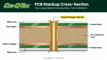
The stack-up itself is straightforward. Components, pads, and traces live on the top and bottom signal layers, with the actual routing split between the two based on where things fit best.
Between them sits the dielectric core, typically FR-4, which provides electrical insulation and the structural rigidity that keeps the board from flexing under normal use. Plated vias punch through this core to carry signals from one side to the other.
A solder mask coats the copper to protect traces from oxidation and prevent solder bridging during assembly. Silkscreen on top of that labels components, test points, and polarity markings for assembly and debugging.
Standard Thickness Considerations
Most 2-layer boards land around 1.6mm (62 mils) thick, the industry default. The broader range typically runs from about 0.4mm to 2.4mm (0.016" to 0.095"), depending on the dielectric material and the mechanical demands of the application.
A few things push thickness in either direction:
- Larger or heavier components may need a thicker board for mechanical support
- Applications with tight enclosure clearance may call for thinner boards
- Dielectric material choice affects both thickness and impedance characteristics
2-Layer PCB Design Rules & Ground Plane Strategy
On a 2-layer board, trace sizing, layer use, and ground strategy do most of the electrical heavy lifting. Trace width isn't a one-size-fits-all number. Power traces generally need to be wider than signal traces because they carry higher continuous current, while signal traces can stay narrow since they're only carrying logic-level current.
Copper weight matters just as much as width. A heavier copper weight (2 oz vs. 1 oz, for example) increases the cross-sectional area of a trace, which lets it carry more current at the same temperature rise.
IPC-2152 treats this as a thermal problem: temperature rise depends on conductor width, thickness, nearby copper, and the board's overall construction, not a fixed width-per-amp rule you can memorize.
Layer allocation on a 2-layer stackup usually follows a simple pattern:
- Dedicate one layer primarily to signal and power routing
- Use the other layer for ground return and component placement
- Keep return paths as short and direct as possible
This shortens the loop between a signal and its return path, which reduces radiated noise and keeps switching behavior more predictable.
Lock component placement early so routing stays clean:
- Group related components together
- Keep high-speed or sensitive traces away from noisy digital lines
- Leave spacing so you don't route yourself into a corner later
Does Your 2-Layer Board Need a Ground Plane?
Short answer: almost certainly, yes. A dedicated ground plane or copper pour helps with EMI control, gives switching circuits a stable reference, and honestly just makes routing easier because you're not hunting for a return path on every net.
When a full plane isn't practical because signal routing eats up too much of the layer, ground gridding (a mesh of ground traces instead of solid copper) is a reasonable compromise. It's not as effective as a solid plane, but it beats scattered, indirect returns.
There are limited scenarios where skipping a ground plane is acceptable:
- Simple DC-only circuits with no switching noise concerns
- Very low-density boards with minimal digital content
- Non-digital analog boards with relaxed EMI requirements
Commercial products almost always need one anyway, since even "simple" designs tend to have a microcontroller or switching regulator somewhere that benefits from a clean reference.
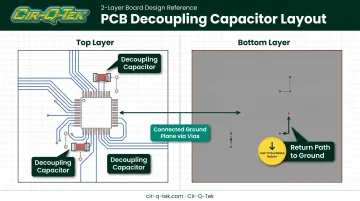
Place decoupling capacitors as close as possible to IC power pins, with a short, low-inductance path to the ground plane. Pair that with a one-return-per-digital-signal rule: each digital signal gets its own clear return path rather than sharing one with unrelated circuits. Ground bounce drops significantly.
2-Layer vs. 4-Layer vs. Single-Layer PCBs: Making the Right Choice
Single-layer boards still matter for context. Single-sided boards route everything on one copper layer, which keeps cost rock-bottom but forces jumper wires or larger board sizes once complexity rises. Double-sided boards add a second routing surface, which is why most designs skip single-layer once more than a handful of components are involved.
The bigger decision is 2-layer vs. 4-layer. A 4-layer stackup adds internal power and ground planes between the two outer signal layers. That change delivers continuous reference planes, shorter return paths, and better EMI performance by default. A 2-layer board has to work hard to approximate those gains with careful layout.
| Factor | 2-Layer | 4-Layer |
|---|---|---|
| Relative cost | Lower | Higher (added materials/lamination) |
| Lead time | Faster in most shops | Slightly longer due to extra steps |
| Routing density | Moderate | High — internal layers free up routing |
| EMI/signal integrity | Good with careful layout | Better by default (continuous planes) |
| Typical applications | Consumer electronics, power supplies, simple analog/digital | High-speed digital, RF, dense BGAs, mixed-signal |
Specific triggers that push a design to 4 layers:
- High-speed interfaces (USB 3.0+, HDMI, high-speed serial links)
- Dense BGAs or fine-pitch components that need internal routing relief
- Strict EMI/EMC compliance requirements
- Controlled impedance requirements for RF or high-speed signals
Converting a 2-layer design to 4 layers is not a simple bolt-on. You need to re-optimize trace widths, via structures, and the stackup itself. Treating the extra layers as an add-on without adjusting the rest of the design usually creates more problems than it solves.
Sierra Circuits estimates that moving from a 2-layer to 4-layer build can increase fabrication cost by roughly 30–40%. Use that range as a starting point when budgeting the upgrade.
Advantages and Disadvantages of 2-Layer PCBs
Advantages:
- Lower fabrication cost than any multilayer alternative
- Faster lead times due to simpler processing
- Easier repair and troubleshooting: both layers are visually accessible
- Lower per-unit cost on large-volume orders
Disadvantages:
- Limited routing density compared to boards with internal layers
- Weaker support for high-speed signals and tight EMI control
- Larger board outline often needed to fit components and routing
Quick guidance: If your design is low-speed, moderate in component count, and cost-driven, a 2-layer board is usually the right call. When you're short on routing space, chasing EMI compliance, or placing fine-pitch BGAs, move up to more layers.
How Much Does a 2-Layer PCB Cost?
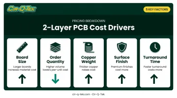
There's no single universal price. Cost depends on how several variables interact for your specific project. The primary drivers include:
- Board size: larger boards consume more panel area and material
- Order quantity: per-unit cost drops as volume increases
- Copper weight: heavier copper costs more to process
- Surface finish: options like HASL, ENIG, or immersion silver carry different price points
- Turnaround time: faster builds typically cost more per unit
2-layer boards remain the most economical PCB option available. The price gap versus 4-layer boards widens further when you add heavier copper or tighter tolerances.
Practical ways to reduce cost:
- Stick to standard panel sizes rather than custom dimensions
- Avoid unnecessarily tight tolerances on trace width or spacing
- Batch prototype runs together instead of ordering piecemeal
Suppliers without rigid minimum order quantities help keep early builds affordable. Cir-Q-Tek, for example, supports orders at any volume—from a handful of prototypes through full production—so you can scale without switching vendors mid-project.
Choosing the Right Manufacturing Partner for Your 2-Layer PCB
Even a straightforward 2-layer design can run into trouble at the fabrication stage if stackup, trace width, or via structures weren't checked against the manufacturer's actual capabilities. A design-for-manufacturability (DFM) review catches those gaps on paper, which is far cheaper than finding them after a production run ships with a defect.
Cir-Q-Tek operates as a one-stop PCB and PCBA sourcing partner built around this kind of early collaboration. Capabilities that matter for 2-layer work include:
- Quick-turn prototypes in 3 days to build and 2 days to ship, so iterations don't stall
- ISO 9001, ISO 13485, and IATF 16949 coverage for medical, automotive, and commercial requirements
- Inline AOI and X-ray inspection through both prototype and volume production
As product lines scale, a single-source partner with CAD design support, parts stocking, and just-in-time delivery removes the juggling of separate vendors for fabrication, assembly, and inventory. That matters more as order volumes grow and the cost of a missed delivery window climbs with them.
Frequently Asked Questions
What is a 2 layer PCB?
A 2-layer PCB is a double-sided board with copper on both the top and bottom layers, connected through plated through-holes (vias). It's the most economical PCB type beyond single-sided boards.
What is the difference between 2 layer and 4 layer PCB?
A 4-layer board adds internal power and ground planes between the two outer signal layers, improving signal integrity and EMI performance. It costs more and takes slightly longer to fabricate than a 2-layer board.
How much does a 2 layer PCB cost?
Cost depends on board size, order quantity, copper weight, and surface finish. Generally, 2-layer boards are the most affordable option once you move past single-sided boards.
Do 2-layer PCBs need a ground plane?
Most 2-layer designs benefit from a ground plane or copper pour for EMI control and simpler routing. Exceptions are rare, mainly simple DC-only or very low-density boards.
Can I convert a 2-layer PCB design to a 4-layer board later?
Yes, but it's not a simple layer addition. You'll need to re-evaluate the stackup, adjust trace widths, and rework via structures to take advantage of the added layers properly.
What is the standard thickness of a 2-layer PCB?
The common standard is 1.6mm (62 mils), though thickness typically ranges from about 0.4 mm to 2.4 mm (0.016" to 0.093") depending on the application and dielectric material.